3Si Security Systems GT83000A ASSET TRACKING AND ALERT DEVICE User Manual GE865 Harware User Guide
3Si Security Systems Inc. ASSET TRACKING AND ALERT DEVICE GE865 Harware User Guide
Contents
- 1. User Manual
- 2. Regulatory Leaflet
- 3. Hardware Guide
Hardware Guide


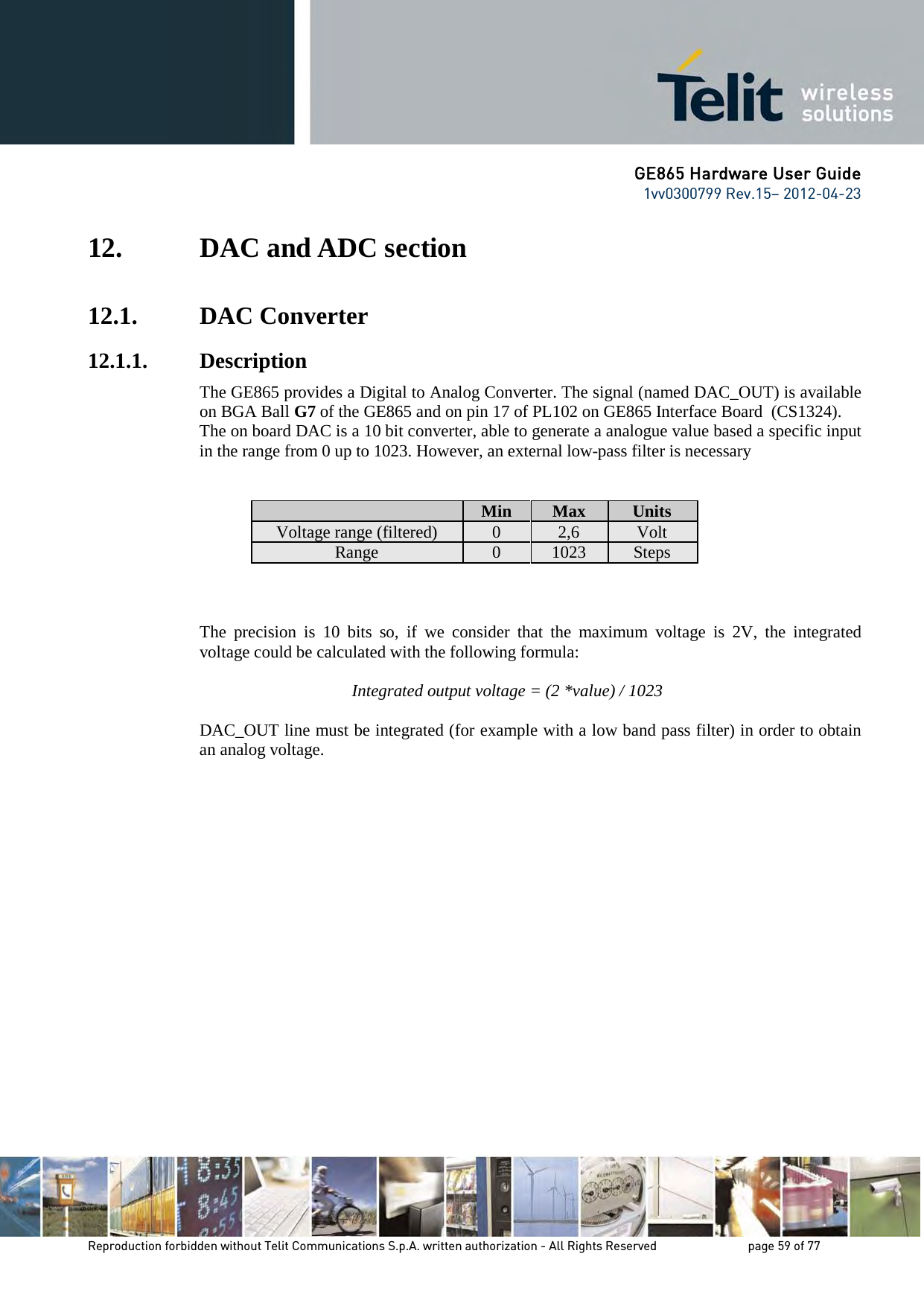
![GE865 Hardware User Guide 1vv0300799 Rev.15– 2012-04-23 Reproduction forbidden without Telit Communications S.p.A. written authorization - All Rights Reserved page 60 of 77 12.1.2. Enabling DAC An AT command is available to use the DAC function. The command is: AT#DAC= [<enable> [, <value>]] <value> - scale factor of the integrated output voltage (0..1023 - 10 bit precision) it must be present if <enable>=1 Refer to SW User Guide or AT Commands Reference Guide for the full description of this function. NOTE: The DAC frequency is selected internally. D/A converter must not be used during POWERSAVING. 12.1.3. Low Pass Filter Example](https://usermanual.wiki/3Si-Security-Systems/GT83000A.Hardware-Guide/User-Guide-1944351-Page-60.png)
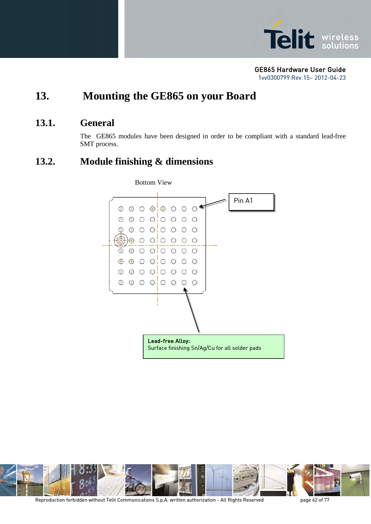

![GE865 Hardware User Guide 1vv0300799 Rev.15– 2012-04-23 Reproduction forbidden without Telit Communications S.p.A. written authorization - All Rights Reserved page 65 of 77 13.6. PCB pad design Non solder mask defined” (NSMD) type is recommended for the solder pads on the PCB. Recommendations for PCB pad dimensions Ball pitch [mm] 2,4 Solder resist opening diameter A [mm] 1,150 Metal pad diameter B [mm] 1 ± 0.05 It is not recommended to place via or microvia not covered by solder resist in an area of 1,6mm diameter around the pads unless it carries the same signal of the pad itself. (see following figure).](https://usermanual.wiki/3Si-Security-Systems/GT83000A.Hardware-Guide/User-Guide-1944351-Page-65.png)
![GE865 Hardware User Guide 1vv0300799 Rev.15– 2012-04-23 Reproduction forbidden without Telit Communications S.p.A. written authorization - All Rights Reserved page 66 of 77 Holes in pad are allowed only for blind holes and not for through holes. Recommendations for PCB pad surfaces: Finish Layer thickness [µm] Properties Electro-less Ni / Immersion Au 3 –7 / 0.05 – 0.15 good solder ability protection, high shear force values The PCB must be able to resist the higher temperatures which are occurring at the lead-free process. This issue should be discussed with the PCB-supplier. Generally, the wettability of tin-lead solder paste on the described surface plating is better compared to lead-free solder paste. 13.7. Solder paste Lead free Solder paste Sn/Ag/Cu It is recommended to use only “no clean” solder paste in order to avoid the cleaning of the modules after assembly.](https://usermanual.wiki/3Si-Security-Systems/GT83000A.Hardware-Guide/User-Guide-1944351-Page-66.png)