B plus B SmartWorx WLNG551 Ethernet Device Adapter User Manual
B&B; Electronics Ethernet Device Adapter
UserManual.wiki
>
B plus B SmartWorx
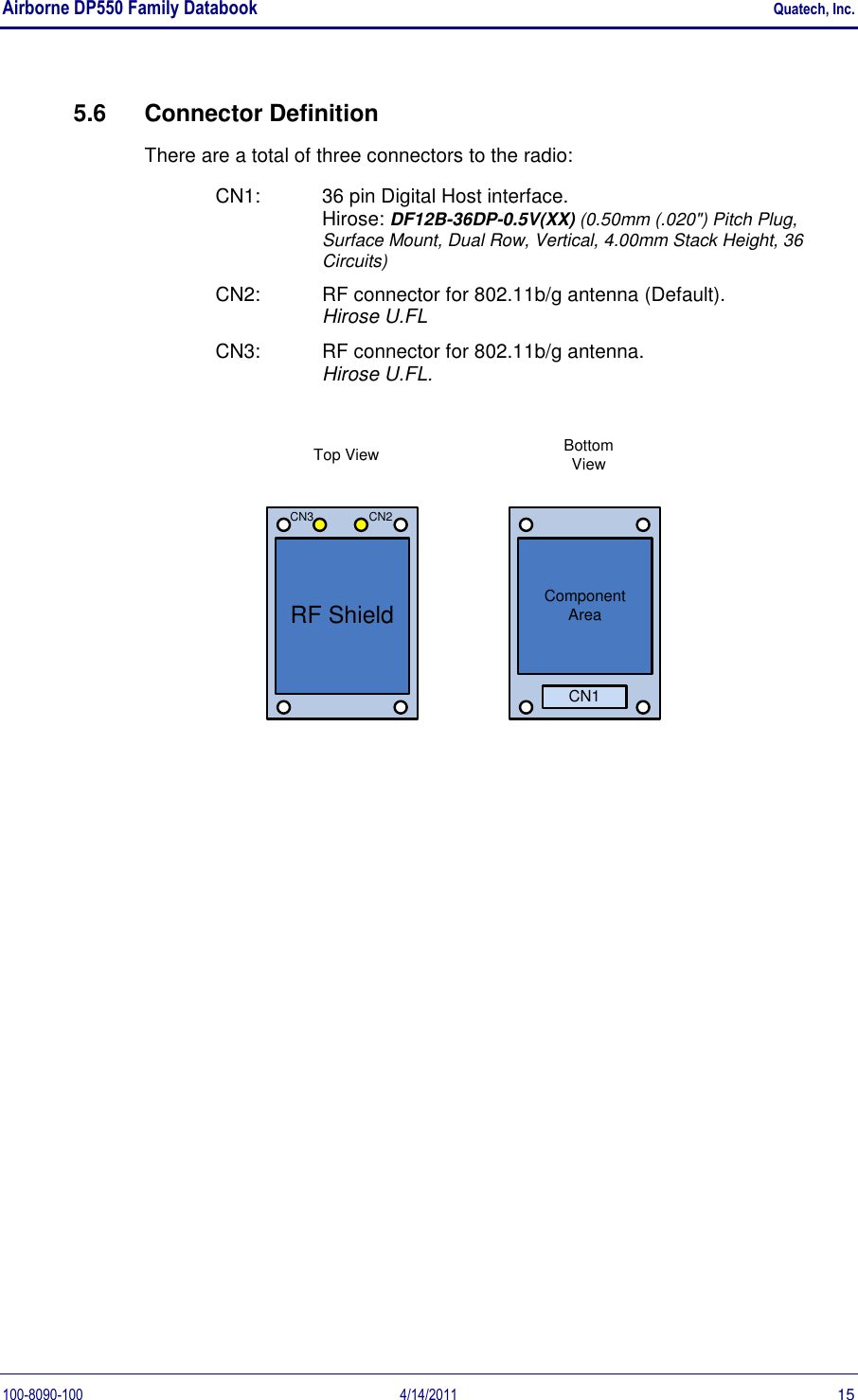
>
WLNG551 User Manual
User Manual
Navigation menu
Upload a User Manual
Namespaces
Wiki Guide
HTML
PDF
Info
Views
User Manual
Discussion / Help
Navigation