Benq AWL700 Wireless Router User Manual ISL3873
Benq Corporation Wireless Router ISL3873
UserManual.wiki
>
Benq
>
AWL700 User Manual
>
users manual 2
Contents
1.
users manual 1
2.
users manual 2
users manual 2
Navigation menu
Upload a User Manual
Namespaces
Wiki Guide
HTML
PDF
Info
Views
User Manual
Discussion / Help
Navigation
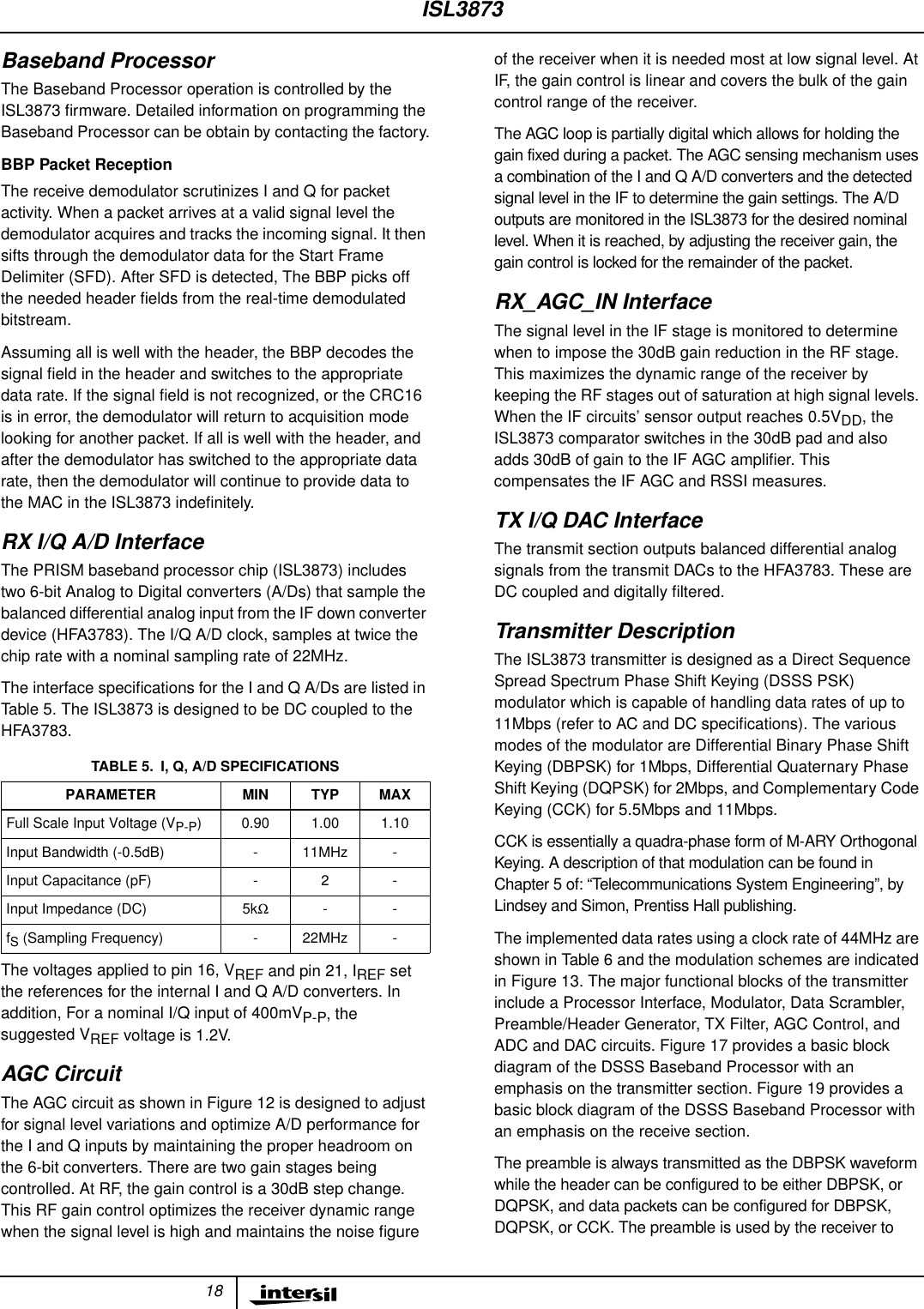
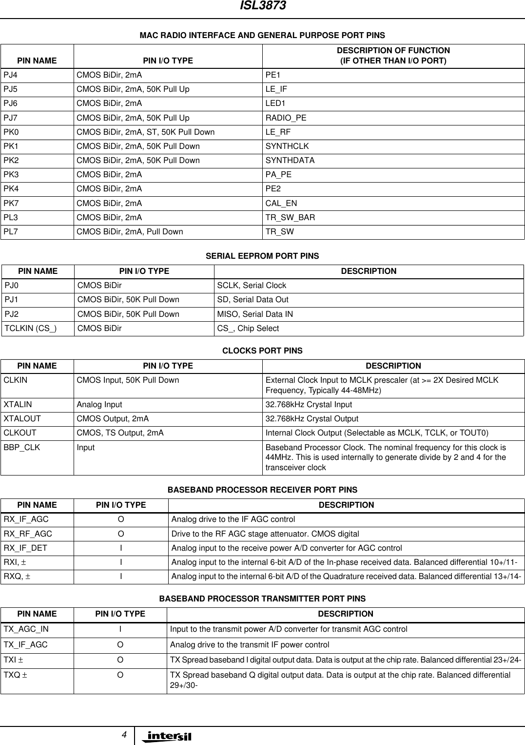
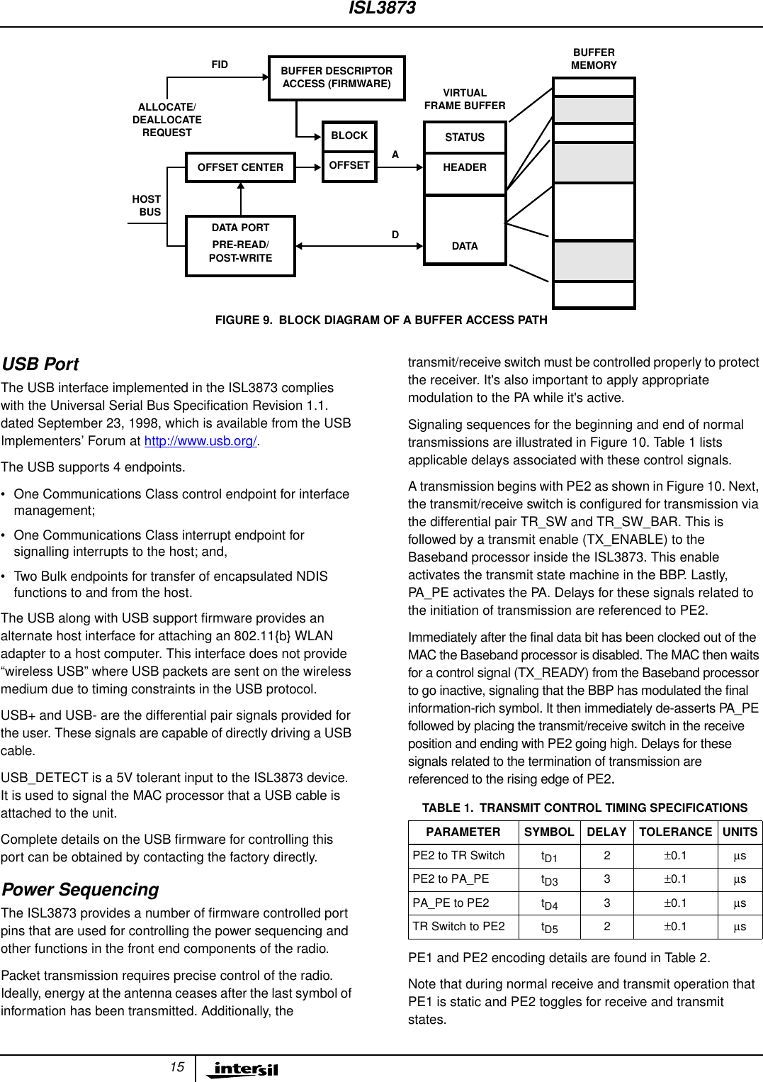
![3ISL3873 Signal DescriptionsHOST INTERFACE PINSPIN NAME PIN I/O TYPE DESCRIPTIONHA0-9 5V tol, CMOS, Input, 50K Pull Down Host PC Card Address Input, Bits 0 to 9HCE1- 5V tol, CMOS, Input, 50K Pull Up Host PC Card Select, Low ByteHCE2- 5V tol, CMOS, Input, 50K Pull Up Host PC Card Select, High ByteHD0-15 5V tol, BiDir, 2mA, 50K Pull Down Host PC Card Data Bus, Bit 0 to 15HINPACK- CMOS Output, 2mA Host PC Card I/O Decode ConfirmationHIORD- 5V tol, CMOS, Input, 50K Pull Up Host PC Card I/O Space Read StrobeHIOWR- 5V tol, CMOS, Input, 50K Pull Up Host PC Card I/O Space Write StrobeHRDY/HIREQ- CMOS Output, 4mA Host PC Card interrupt Request (I/O Mode), also used as PC CardReady (Memory Mode) output which is asserted to indicate cardinitialization is completeHOE- 5V tol, CMOS, Input, 50K Pull Up Host PC Card Memory Attribute Space Output EnableHREG- 5V tol, CMOS, Input, 50K Pull Up Host PC Card Attribute Space SelectRESET 5V tol, CMOS, ST Input, 50K Pull Up Hardware Reset. Self-asserted by internal pull-up at power-on. Clocksignal CLKIN or XTALIN must be available before negation of Reset.Value of MD[15..0] copied to MDIR[15..0] and various control registerbits on the first MCLK following release of ResetHSTSCHG- CMOS Output, 4mA Host PC Card Status ChangeHWAIT- CMOS Output, 4mA Host Wait, asserted to indicate data transfer not complete and to forceforce host bus wait statesHWE- 5V tol, CMOS Input, 50K Pull Up Host PC Card Memory Attribute Space Write EnableUSB INTERFACE PINSPIN NAME PIN I/O TYPE DESCRIPTIONUSB+ CMOS BiDir, 2mA, (Also USB Transceiver) USB, MBUS Address Bit 20, or I/O as PL5USB- CMOS BiDir, 2mA, (Also USB Transceiver) USB, MBUS Address Bit 21, or I/O as PL6USB_DETECT Input, 5V tolerant, pull-down Sense USB VBUS to indicate cable attachmentMEMORY INTERFACE PINSPIN NAME PIN I/O TYPE DESCRIPTIONMUBE- / MA0 /MWEH-CMOS TS Output, 2mA MBUS Upper Byte Enable for x16 Memory; MBUS Address Bit 0 (byte)for x8 Memory; High Byte Write Enable for 2 x8 MemoriesMA1-18 CMOS TS Output, 2mA MBUS Address Bits 1 to 18PL4-MA19 CMOS BiDir, 2mA MBUS Address Bit 19MLBE- CMOS TS Output, 2mA, 50K Pull Up MBUS Lower Byte Enable, or I/O as PM2MOE- CMOS TS Output, 2mA Memory Output EnableMWE- / MWEL- CMOS TS Output, 2mA Low (or only) Byte Memory Write EnableRAMCS- CMOS TS Output, 2mA RAM SelectNVCS- CMOS TS Output, 2mA NV Memory SelectMD0-7 5V tol, CMOS, BiDir, 2mA, 100K Pull Up MBUS Low Data Byte, Bits 0 to 7MD8-15 5V tol, CMOS, BiDir, 2mA50K Pull-Downs on MD15, MD14, MD13, MD11,MD10, MD0950K Pull-Ups MD12, MD08MBUS High Data Byte, Bits 8 to 15Default power up states are defined by pull-up and pull-down internalresistors as shown. Device defaults to external EEPROM for boot upmode. Using external 10K resistors, configure these pins according toTable 4 to change power-up configurationISL3873](https://usermanual.wiki/Benq/AWL700.users-manual-2/User-Guide-260650-Page-3.png)
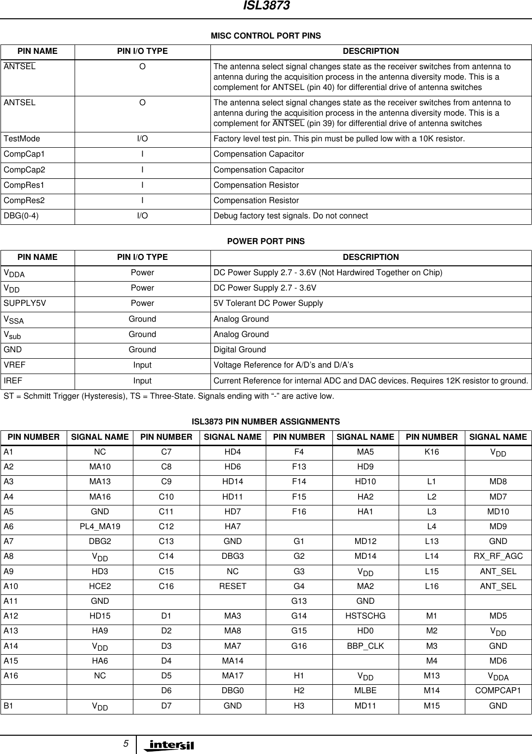
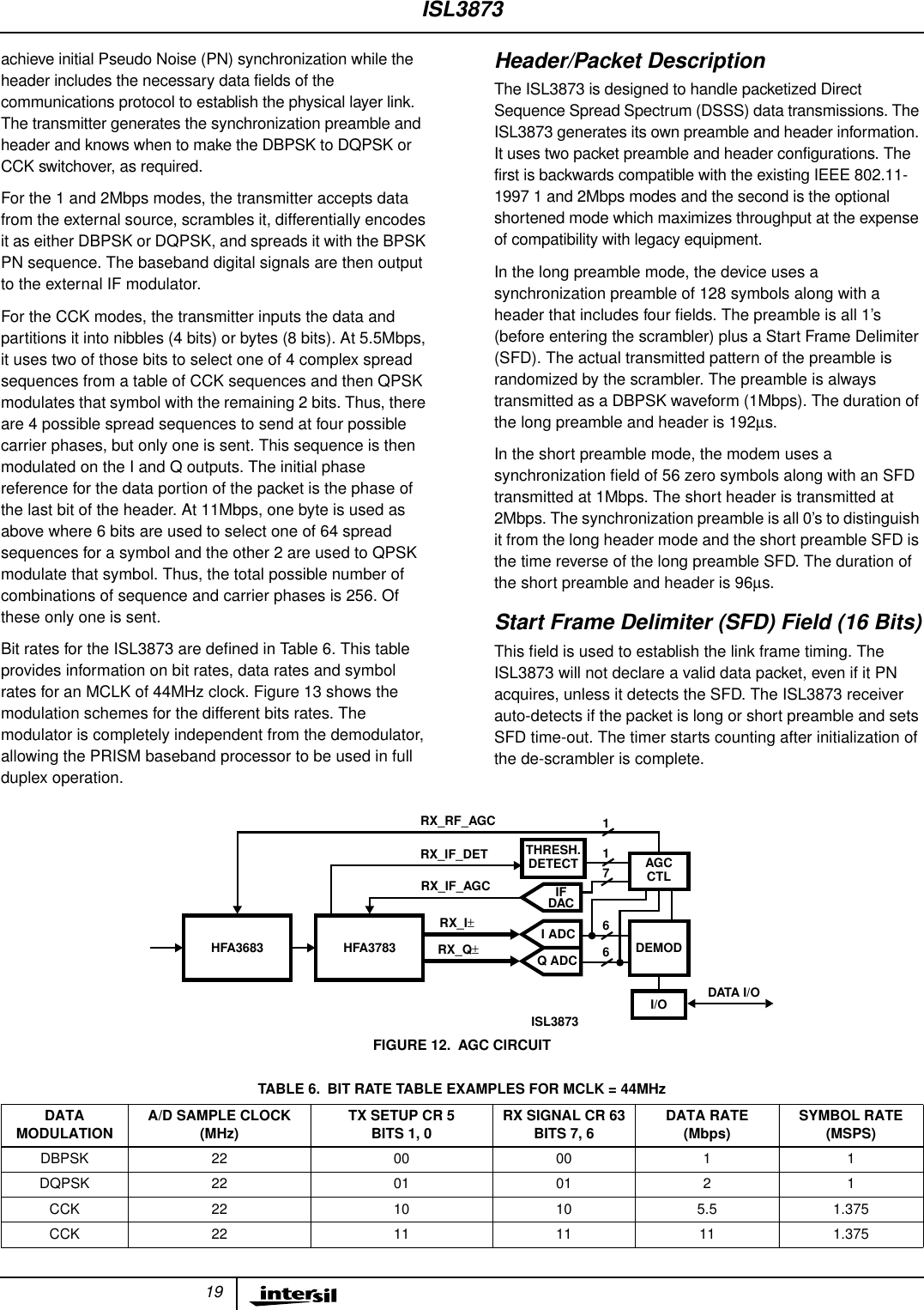
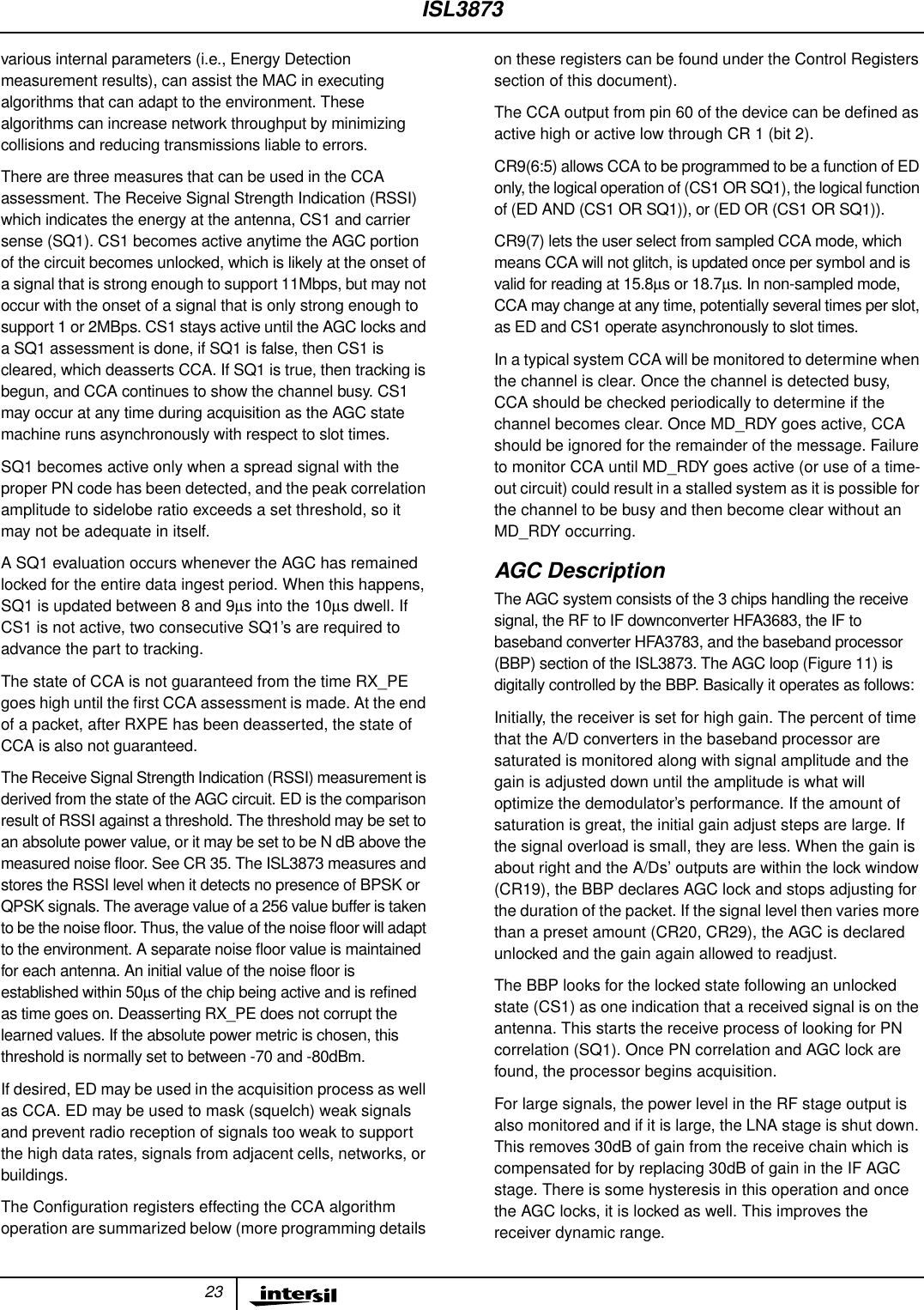
![9WaveformsFIGURE 1. EXTERNAL MEMORY READ TIMINGFIGURE 2. EXTERNAL MEMORY WRITE TIMINGFIGURE 3. SYNTHESIZERADDRESSMA(17..1)tH1tE1tS2tH2RAMCS_MOE_MD(15..0)tS1tD1ADDRESSMA(17..1)tH5tH4tS4tS3tH3RAMCS_MWE_MD(15..0)tS5SYNTHCLKSYNLESPCSPWRSYNTHDATAtH1 tL1tCYCtD1 tD2tD3D[n] D[n -1] D[n -2] D[2] D[1] D[0]ISL3873](https://usermanual.wiki/Benq/AWL700.users-manual-2/User-Guide-260650-Page-9.png)
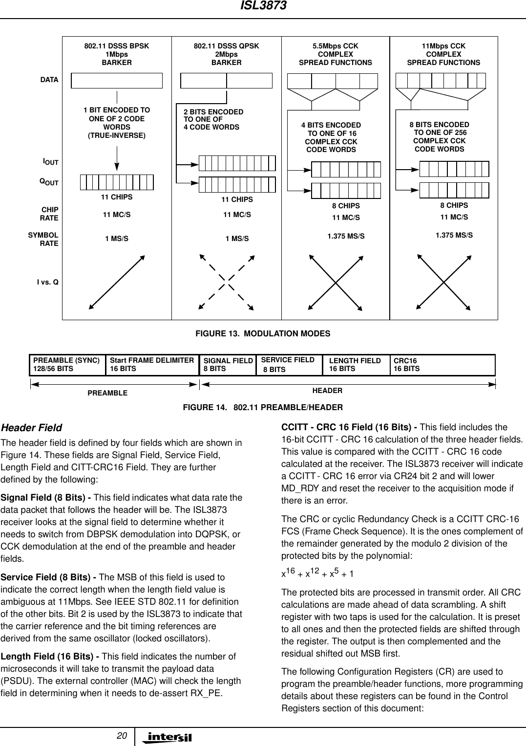
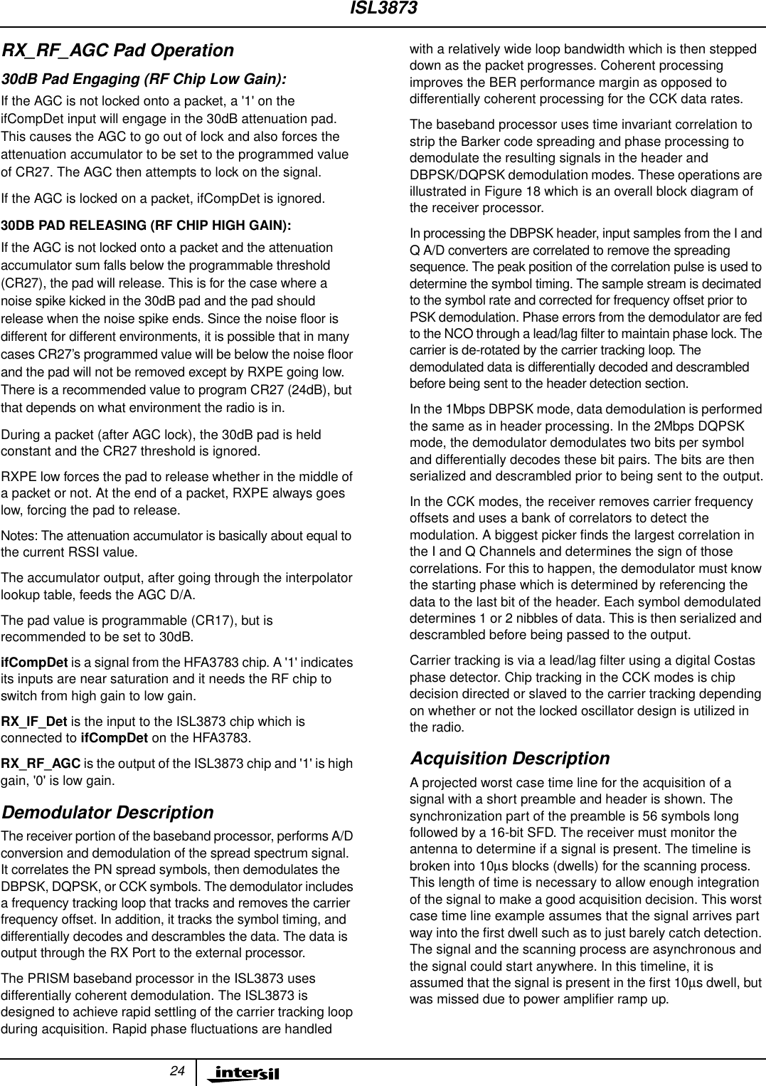
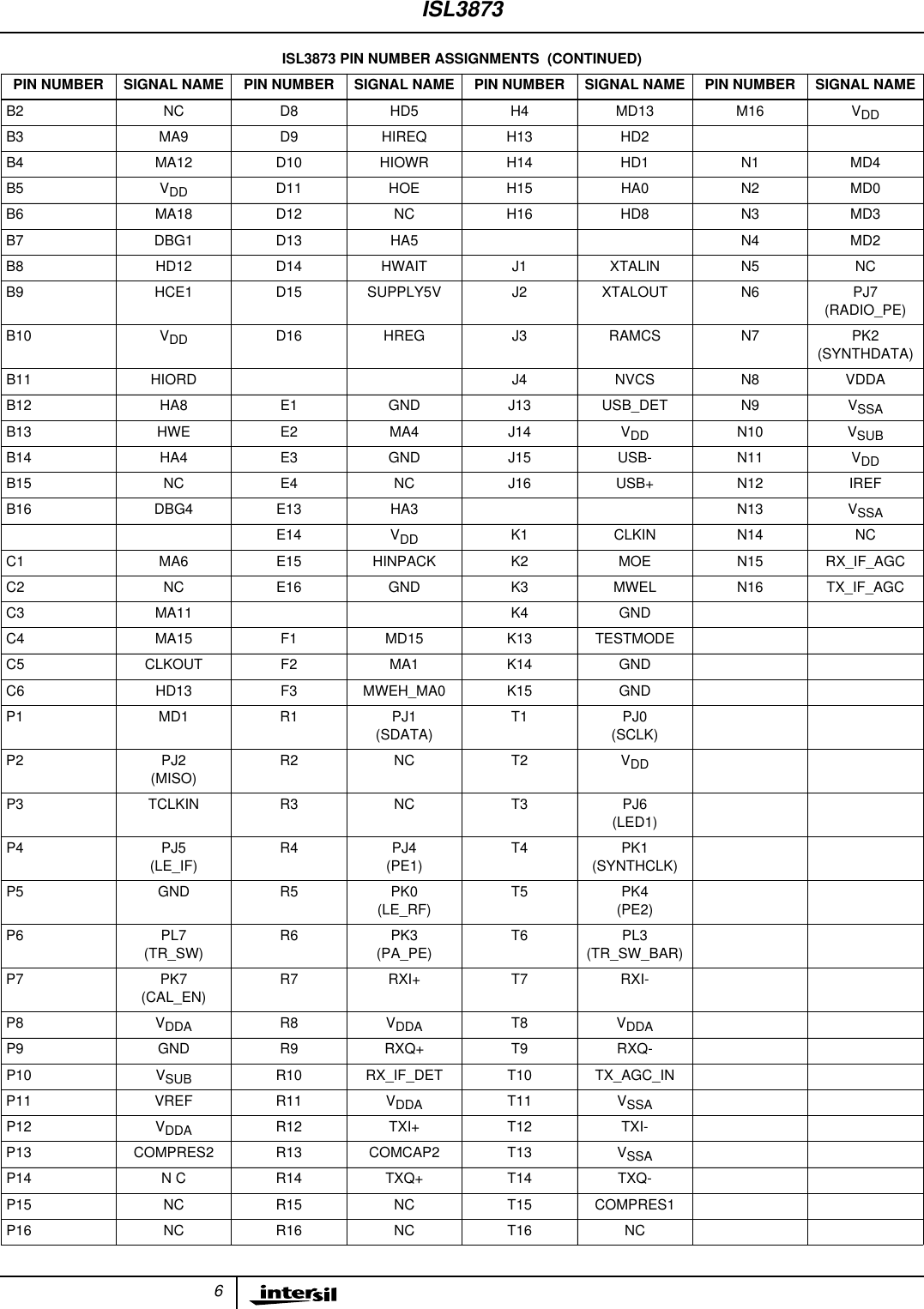
![10FIGURE 4. PC CARD IO READ 16FIGURE 5. PC CARD IO WRITE 16Waveforms (Continued)HA[15:0]HREG-HCE(1, 2) -HIORD-HINPACK-HWAIT-HD[15:0]tSUREGISUCEtHREGtHCEtWIORDtDIORDtDFINPACKtSUAtDFWT tDRWTtHIORDtDRINPACKtHAtWWTHA[15:0]HREGN-HCE (1, 2) -HIOWR-HWAIT-HD[15:0]tSUREG tHREGtHAtHCEtSUCEtSUAtDFWTtSUIOWR tWWT tHIOWRtDRIOWRtWIOWRtDRINPACKISL3873](https://usermanual.wiki/Benq/AWL700.users-manual-2/User-Guide-260650-Page-10.png)
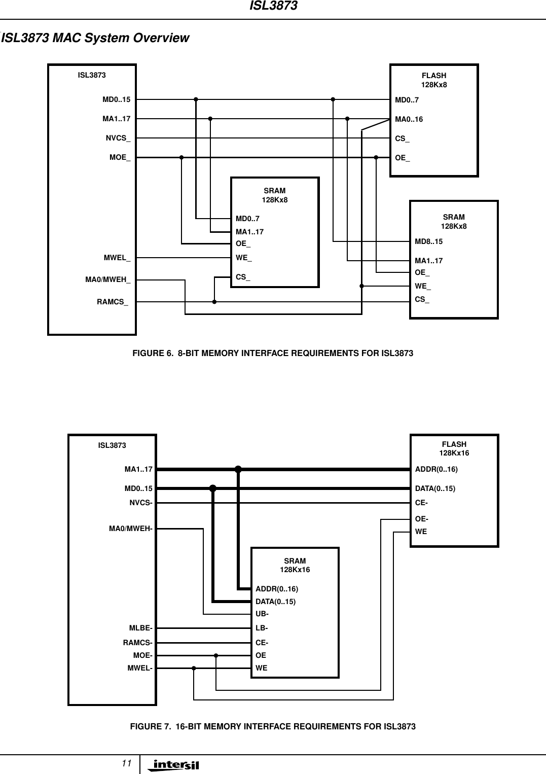
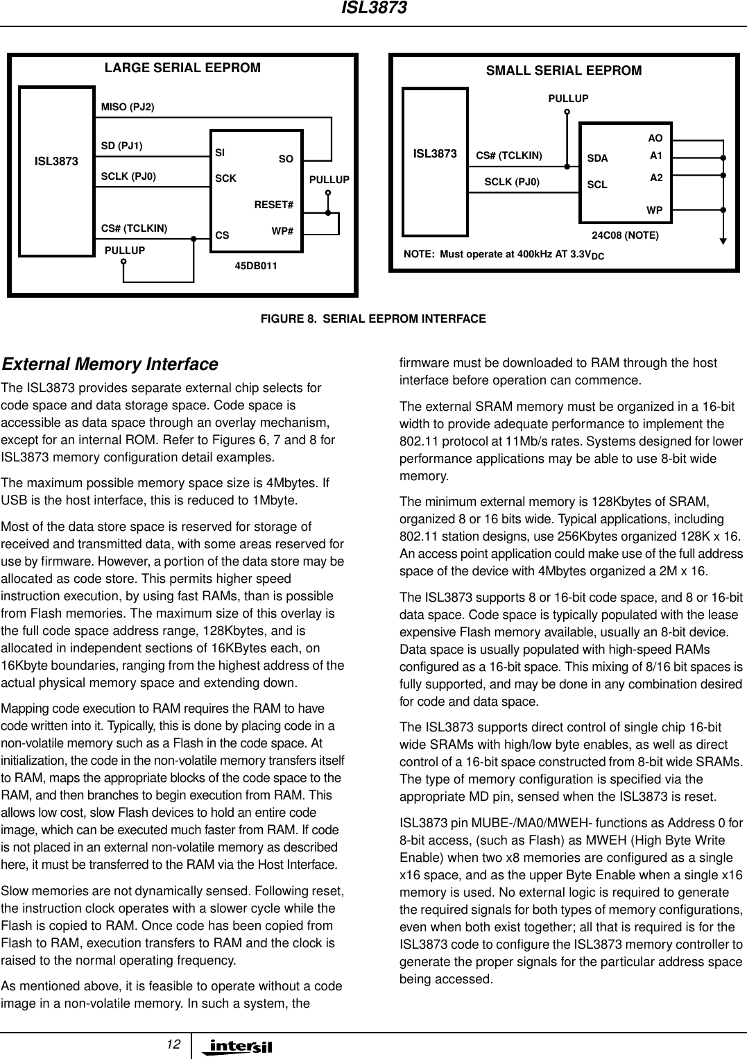
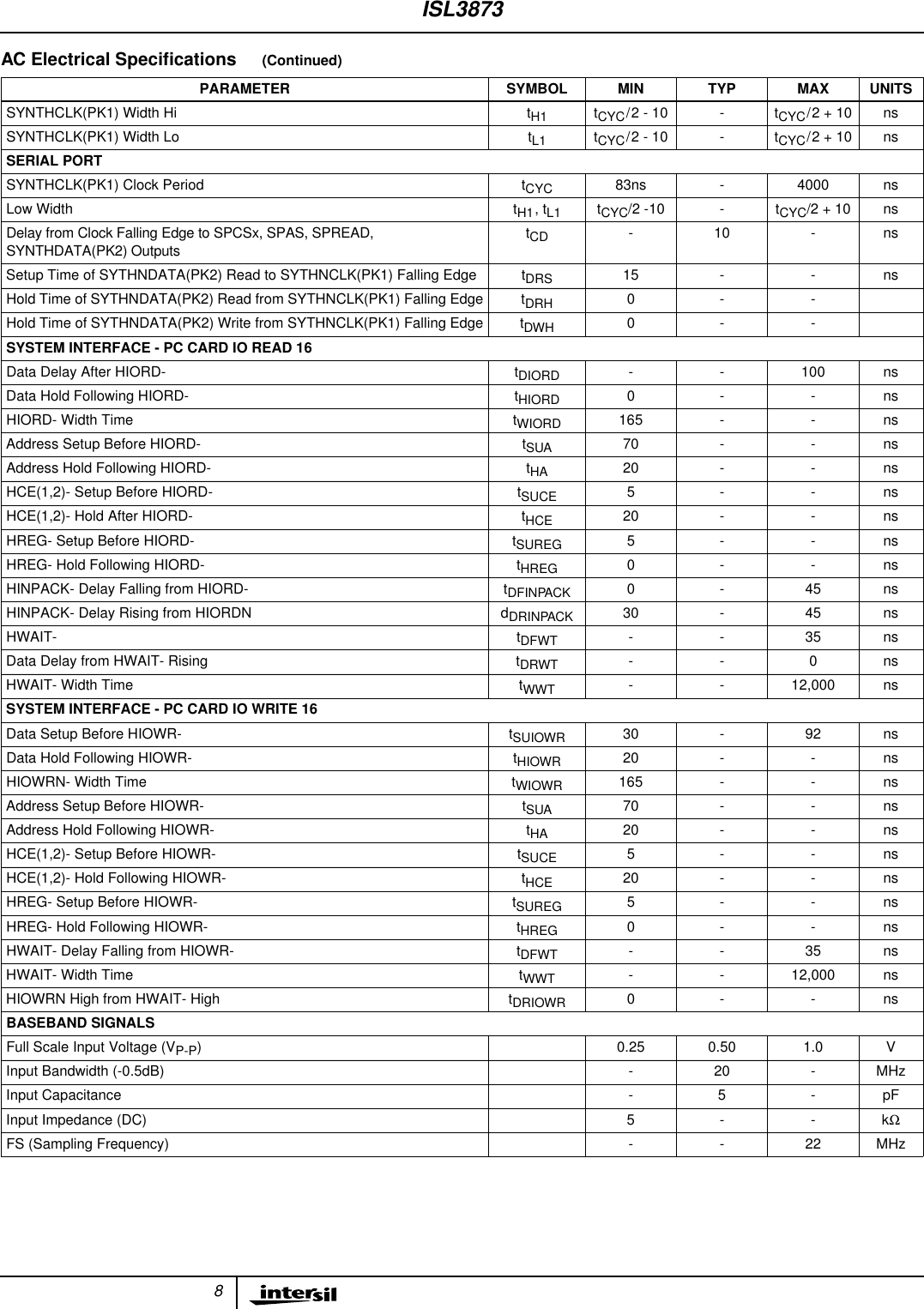
![13For 8-bit spaces, the ISL3873 dynamically configures pinMUBE-/MA0/MWEH- cycle-by-cycle as the address LSB.MWEL-/MWE- is the only write control, and MOE- is the readoutput enable.For 16-bit spaces constructed from 8-bit memories, theISL3873 dynamically configures pin MUBE-/MA0/MWEH-cycle-by-cycle as the high byte write enable, MWEL- as the lowwrite enable signal, and MOE- as the read output enable.For 16-bit spaces constructed from single-chip x16memories (such as SRAMs), the ISL3873 dynamicallyconfigures pin MUBE_/MA0/MWEH- cycle-by-cycle as theupper byte enable. Pin MLBE- is connected as the low byteenable, MWEL-/MWE- is the write control, and MOE- is theread output enable.These memory implementations require no external logic.The memory spaces may each be constructed from any typeof memory desired. The only restriction is that a singlememory space must be constructed from the same type ofmemory; for example, data space may not use both x8 andx16 memories, it must be all x8, or all x16. This restrictiondoes not apply across memory spaces; e.g., code space mayuse a x8 memory and data space a single x16 memory, orcode space two x8 memories and data space a single x8memory.Serial EEPROM InterfaceThe ISL3873 contains a small on-chip ROM firmware whichwas added to allow the CIS or CIS plus firmware image to betransferred from an off-chip serial non-volatile memory deviceto RAM after a system reset. This allows a system configurationwithout a parallel Flash device. The operating frequency of theserial port is 400kHz with a voltage of 3.3V. Refer to Figure 8 foradditional details on configuring the serial memory to theISL3873. The Power On Reset Configuration section in thisdocument provides additional details on memory selection andcontrol after a Reset condition.PC Card InterfacePC Card Physical InterfaceThe Host interface is compatible to the PC Card 95 Standard(PCMCIA v2.1). The ISL3873 Host Interface pins connectdirectly to the correspondingly named pins on the PC Cardconnector with no external components (other than resistors)required. The ISL3873 operates as an I/O card using lessthan 64 octet locations. Reads and writes to internal registersand buffer memory are performed by I/O accesses. Attributememory (256 octets) is provided for the CIS table which islocated in external memory. Common memory is not used.The following describes specific features of various pins:HA[9:0]Decoding of the system address space is performed by theHCEx-. During I/O accesses HA[5:0] decode the register.HA[9:6] are ignored when the internal HAMASK register isset to the defaults used by the standard firmware. Duringattribute memory accesses HA[9:1] are used.HD[15:0]The host interface is primarily designed for word accesses,although all byte access modes are fully supported. SeeHCE1-, HCE2- for a further description. Note that attributememory is specified for and operates with even bytes accessesonly.HCE1-, HCE2-The PC Card cycle type and width are controlled with the CEsignals. Word and Byte wide accesses are supported, usingthe combinations of HCE1-, HCE2-, and HA0 as specified inthe PC Card standard.HWE-, HOE-HOE- and HWE- are only used to access attribute memory.Common Memory, as specified in the PC Card standard, isnot used in the ISL3873. HOE- is the strobe that enables anattribute memory read cycle. HWE- is the correspondingstrobe for the attribute memory write cycle. The attributespace contains the Card Information Structure (CIS) as wellas the Function Configuration Registers (FCR).HIORD-, HIOWR-HIORD- and HIOWR- are the enabling strobes for registeraccess cycles to the ISL3873. These cycles can only beperformed once the initialization procedure is complete andthe ISL3873 has been put into IO mode.HREG-This signal must be asserted for I/O or attribute cycles. Acycle where HREG- is not asserted will be ignored as theISL3873 does not support common memory.HINPACK-This signal is asserted by the ISL3873 whenever a valid I/Oread cycle takes place. A valid cycle is when HCE1-, HCE2-,HREG-, and HIORD- are asserted, once the initializationprocedure is complete.HWAIT-Wait states are inserted in accesses using HWAIT-. The hostinterface synchronizes all PC Card cycles to the internalISL3873 clock. The following wait states should be expected:Direct Read or Write to Hardware Register• 1/2 to 1 MCLK assertion of HWAIT- for internalsynchronization.Write to Memory Mapped Register, Buffer Access Path,or Attribute Space (Post-Write)• The data required for the write cycle will be latched andtherefore only the synchronizing wait state will occur.• Until the queued cycle has actually written to the memory,any subsequent access by the Host will result in a WAIT.ISL3873](https://usermanual.wiki/Benq/AWL700.users-manual-2/User-Guide-260650-Page-13.png)
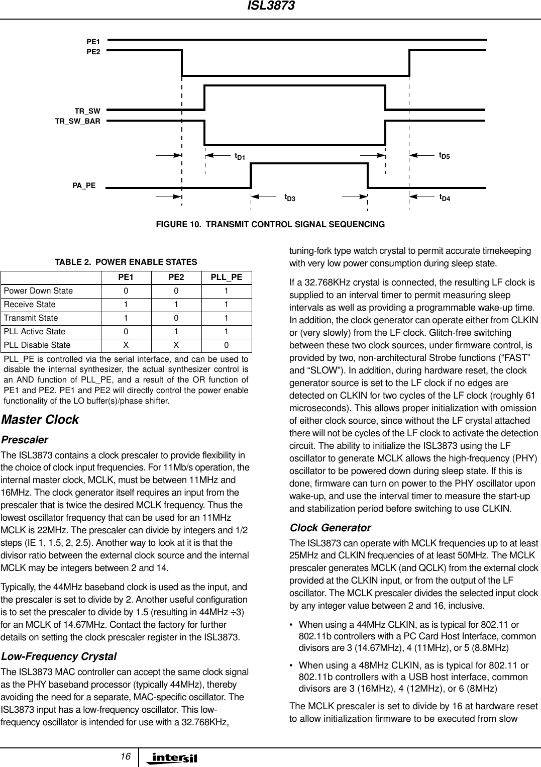
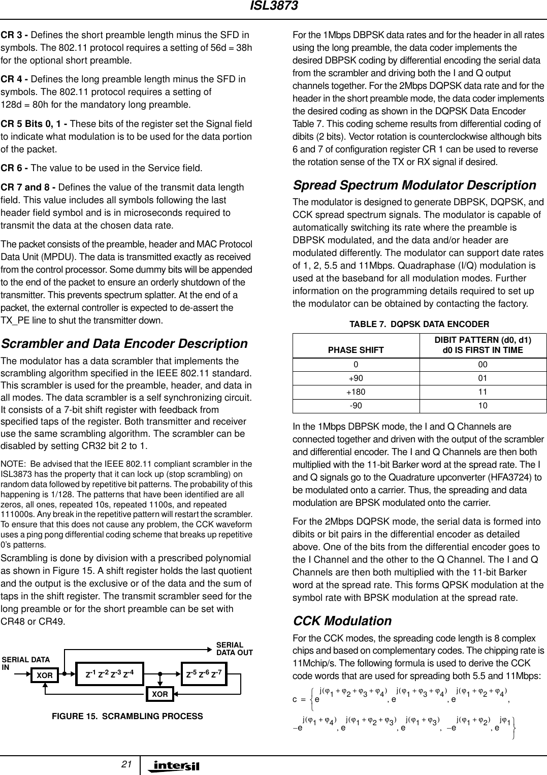
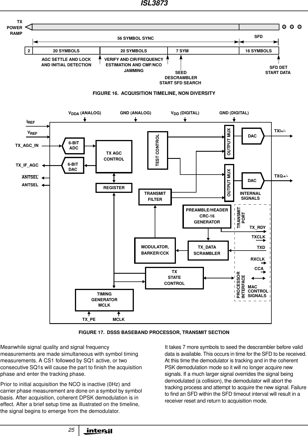
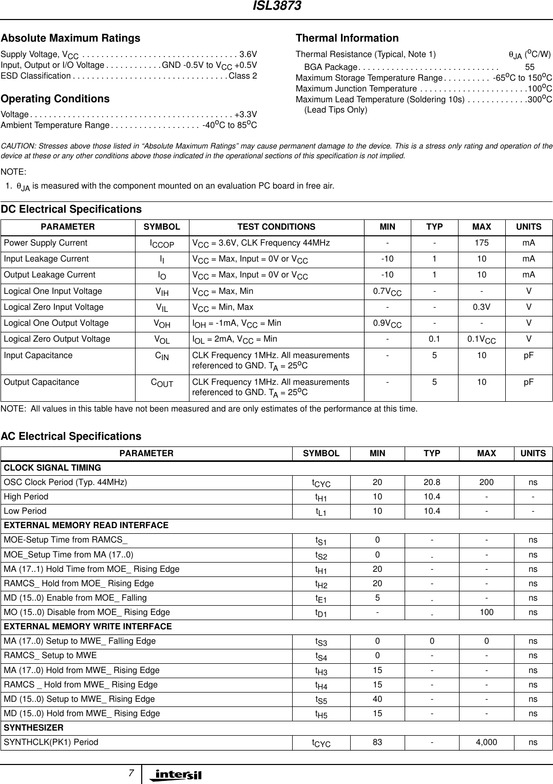
![17memory devices at any CLKIN frequency. The MCLKprescaler generates glitch free output when the divisor ischanged. This allows firmware to change the MCLKfrequency during operation, which is especially useful toselectively reduce operating speed, thereby conservingpower, when full speed processing is not required.Power On Reset ConfigurationPower On Reset is issued to the ISL3873 with the RESETpin or via the soft reset bit, SRESET, in the ConfigurationOption Register (COR, bit 7). RESET originates from theHOST system which applies RESET for at least 0.01ms afterVCC has reached 90% of its end value (see PC-Cardstandard, Vol. 2, Ch. 4.12.1).The MD[15:8] pin values are sampled during RESET orSoftware Reset (SRESET). These pins have internal 50Kresistors. External pull-up or pull-down resistors (typically10kΩ) are used for bits which need to be configureddifferently than the default.Table 3 summarizes the effect per pin. Table 4 provides theMD15 and MD14 bit values required to allow the ISL3873 touse Serial EEPROM option.MD[11], StrIdle, has no equivalent functionality in any controlregister. When asserted at reset, it will inhibit firmwareexecution. This is used to allow the initial download offirmware in “Genesis Mode”. See the Hardware ReferenceManual for more details. The latch is cleared when theSoftware Reset, SRESET, COR(7) is active.XTALINXTALOUTX1C1C2FIGURE 11. 32.768kHz CRYSTAL10MΩ22pF4700pFTABLE 3. INITIALIZATION STRAPPING OPTIONS ON MBUS DATA PINSBITS NAME DEFAULT FUNCTION15:14 NVtype[1:0] 30 Indicates type of serial NV memory to be read by initialization firmware in on-chip ROM.Up to 8 NV device types can be encoded with (StrIdle or NVtype). If StrIdle = 0, NV memory holds a firmwareimage, and NVtype identifies 1 of 4 “large” (. = 128Kb) types. If StrIdle = 1, the NV memory just holds the CIS,and NVtype identifies 1 of 4 “small” (< = 8Kb) types.13 SHIenable 0 Use the Serial Host Interface (USB), and disable all PC Card functions except attribute space, for access to theCOR and HCR for firmware debugging support. When = 0, use the Parallel Host Interface (PC Card or ISA).12 4Wire 1 Use 4-wire interface to SRAM (CS-, OE-, WEH-, WEL-) the ISL3873 x8 SRAMs. When = 0 selects 5-wireinterface for use with x16 SRAM (CS-, OE-, WE-, UBE-, LBE-).11 StrIdle 0 Start idle (wait for download from PC Card host interface).10 Mem16 0 RAM and NV space at startup is x 16. When = 0 RAM and NV space at startup is x 8. If starting from off-chip NVmemory this setting must indicate the width of the startup Flash Memory. During initialization, firmware can setseparate widths or RAM and NV space in the Memory Control Register.9 NVds 0 Disable mapping of off-chip control store to NV space (hence map off-chip control store to RAM space). When= 0 off-chip control store is mapped to NV memory8 ROMds 1 Disable on-chip control store ROM. When = 0 enable on-chip control store ROM.7 ISAmode 0 Set host interface control signals and address decoding for PC card. When = 1 set host interface signals andaddress decoding is for ISA bus, with all registers in I/O space and attribute space disabled. To use ISA mode,PHIenable must be = 1 to enable a parallel host interface.6 FCRinIO 0 Enable I/O space decoding for the physical FCRs. When = 1, the COR, CSR, and PRR registers are accessibleat I/O space offsets 0x40, 0x42, and 0x44 respectively. When = 0 these registers are only accessible in attributespace. This bit is ignored when PHIenable = 0, and is overridden (forced = 1) when ISAmode =1. FCRinIO = 1is useful for PC Card operation (PHIenable = 1, ISAmode = 0) to allow non-OS software to access the COR/HCRin OS environments where the system software does not permit application software to access attribute space.b5:0 Spare 0 x 00 Not assigned.a. FCRinIO = 1 forces HAMASK [0] = 1 to expand I/O space decoding from 0 x 40 to 0 x 80 bytes.TABLE 4. SERIAL EEPROM SELECTIONMD15 MD14 DEVICE TYPE FUNCTION0 0 AT45DB011 Large Serial Device used to transfer firmware to SRAM0 1 24C08 (Note) Small Serial Device which contains only CIS. MAC goes idle after loading CIS and waits for host.1 X None Modes not supported in firmware at this time. Consult factory for additional device types added.NOTE: The operating frequency of the serial port is 400kHz with a voltage of 3.3V.ISL3873](https://usermanual.wiki/Benq/AWL700.users-manual-2/User-Guide-260650-Page-17.png)