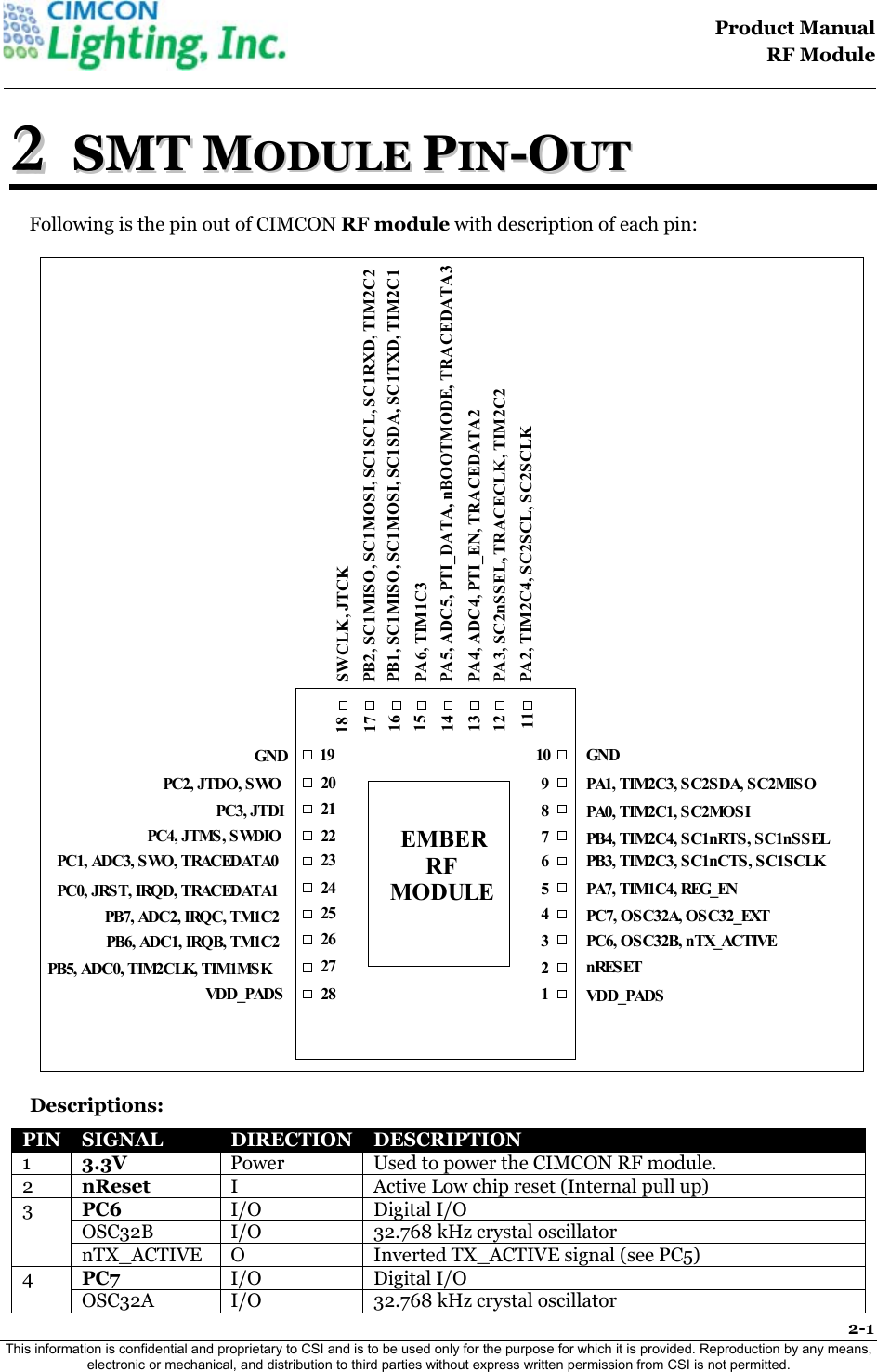
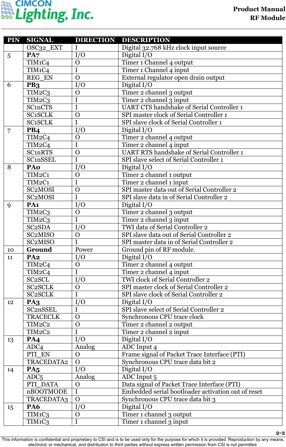
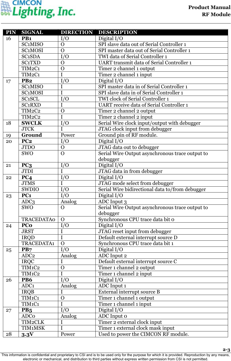
CIMCON Lighting CIM35X1 CIMX1PRO RF MODULE User Manual
CIMCON Lighting, Inc. CIMX1PRO RF MODULE
UserManual.wiki
>
CIMCON Lighting
>
CIM35X1 User Manual
User Manual
Navigation menu
Upload a User Manual
Namespaces
Wiki Guide
HTML
PDF
Info
Views
User Manual
Discussion / Help
Navigation
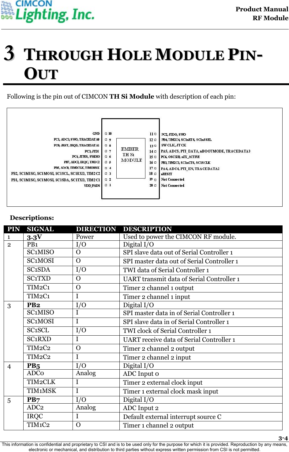
![Product Manual RF Module 4-1 This information is confidential and proprietary to CSI and is to be used only for the purpose for which it is provided. Reproduction by any means, electronic or mechanical, and distribution to third parties without express written permission from CSI is not permitted. 44 CCOONNFFIIGGUURRAATTIIOONN IINNFFOORRMMAATTIIOONN 4.1. Absolute Maximum Ratings of RF Module The following table provides maximum ratings of RF Module: Sr. No. Parameter Symbol Absolute Maximum ratings Unit 1 Supply Voltage Vcc -0.3 to +3.6 VDC 2 Voltage on any GPIO including nReset and JCLK VIN -0.3 to Vcc+0.3 VDC 3 Voltage on any GPIO [PA4, PA5, PB5, PB6, PB7, PC1] when used as input to ADC VIN -0.3 to +2.0 VDC 4 Storage Temperature Range Tstg -40 to +105 ‘C 5 Operating Temperature Range Top -40 to +85 ‘C 6 ESD on any pin (HBM) Vhbm +/-2 KV 7 ESD on RF port (CDM) Vcdm +/-225 V 8 Moisture Sensitivity Level (MSL) MSL3 9 Reflow Temperature Treflow Refer in next pages 4.2. Recommended Operating Conditions Sr. No Parameter Symbol Recommended Operating Conditions Unit 1 Supply Voltage Vcc 2.1 to 3.6 VDC 2 Operating frequency Fin 2405 to 24 MHz 3 Operating Temperature Top -40 to +85’C ‘C 4.3. DC Electrical Characteristics Parameter Test Conditions Min. Typical Max Unit Voltage supply 2.1 3.6 VDC Low Schmitt switching threshold VSWIL Schmitt input threshold going from high to low 0.42 x VDD_PADS 0.50 x VDD_PADS High Schmitt switching threshold VSWIH Schmitt input threshold going from low to high 0.62 x VDD_PADS 0.80 x VDD_PADS V Input current for logic 0 IIL -0.5 uA Input current for logic 1 IIH +0.5 uA Input pull-up resistor value RIPU 24 29 34 kΩ](https://usermanual.wiki/CIMCON-Lighting/CIM35X1/User-Guide-1927406-Page-11.png)
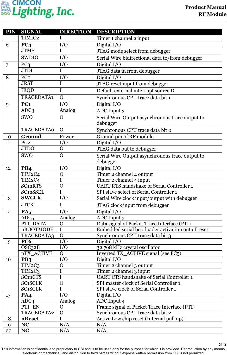
![Product Manual RF Module 4-2 This information is confidential and proprietary to CSI and is to be used only for the purpose for which it is provided. Reproduction by any means, electronic or mechanical, and distribution to third parties without express written permission from CSI is not permitted. Parameter Test Conditions Min. Typical Max Unit Input pull-down resistor value RIPD 24 29 34 kΩ Output voltage for logic 0 VOL (IOL = 4 mA for standard pads, 8 mA for high current pads) 0 0.18 x VDD_PADS V Output voltage for logic 1 VOH (IOH = 4 mA for standard pads, 8 mA for high current pads) 0.82 x VDD_PADS VDD_PADS V Output source current (standard current pad) IOHS 4 mA Output sink current (standard current pad) IOLS 4 mA Output source current high current pad: PA6, PA7, PB6, PB7, PC0 IOHH 8 mA Output sink current high current pad: PA6, PA7, PB6, PB7, PC0 IOLH 8 mA Total output current (for I/O Pads) IOH + IOL 40 mA 4.4. Power Settings for Regulatory Compliance Because of the high gain of the frontend module output power of up to 24dBm can be achieved When the antenna gain is included then the output power of the EM357 transceivers needs to be reduced for regulatory compliance. The following tables list the maximum permitted power setting for the different antenna types listed. This is the power out of the EM357 chip, and the power delivered to the antenna will be higher by the gain of the PA. settxpower P (set the channel power) UFL Antenna Unit • Channel 11: P = -5 [dBm] • Channel 18: P = -5 [dBm] • Channel 25: P = -7 [dBm] Fixed Antenna Unit • Channel 11: P = -3 [dBm] • Channel 18: P = -3 [dBm] • Channel 25: P = -3 [dBm]](https://usermanual.wiki/CIMCON-Lighting/CIM35X1/User-Guide-1927406-Page-12.png)