Cohda Wireless MK5OBU MK5 DSRC RADIO ROADSIDE UNIT User Manual
Cohda Wireless Pty Ltd. MK5 DSRC RADIO ROADSIDE UNIT
UserManual.wiki
>
Cohda Wireless
>
MK5OBU User Manual
User Manual
Navigation menu
Upload a User Manual
Namespaces
Wiki Guide
HTML
PDF
Info
Views
User Manual
Discussion / Help
Navigation
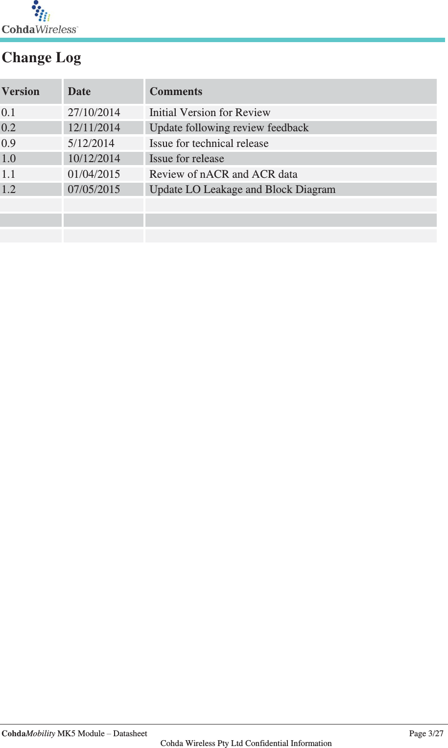
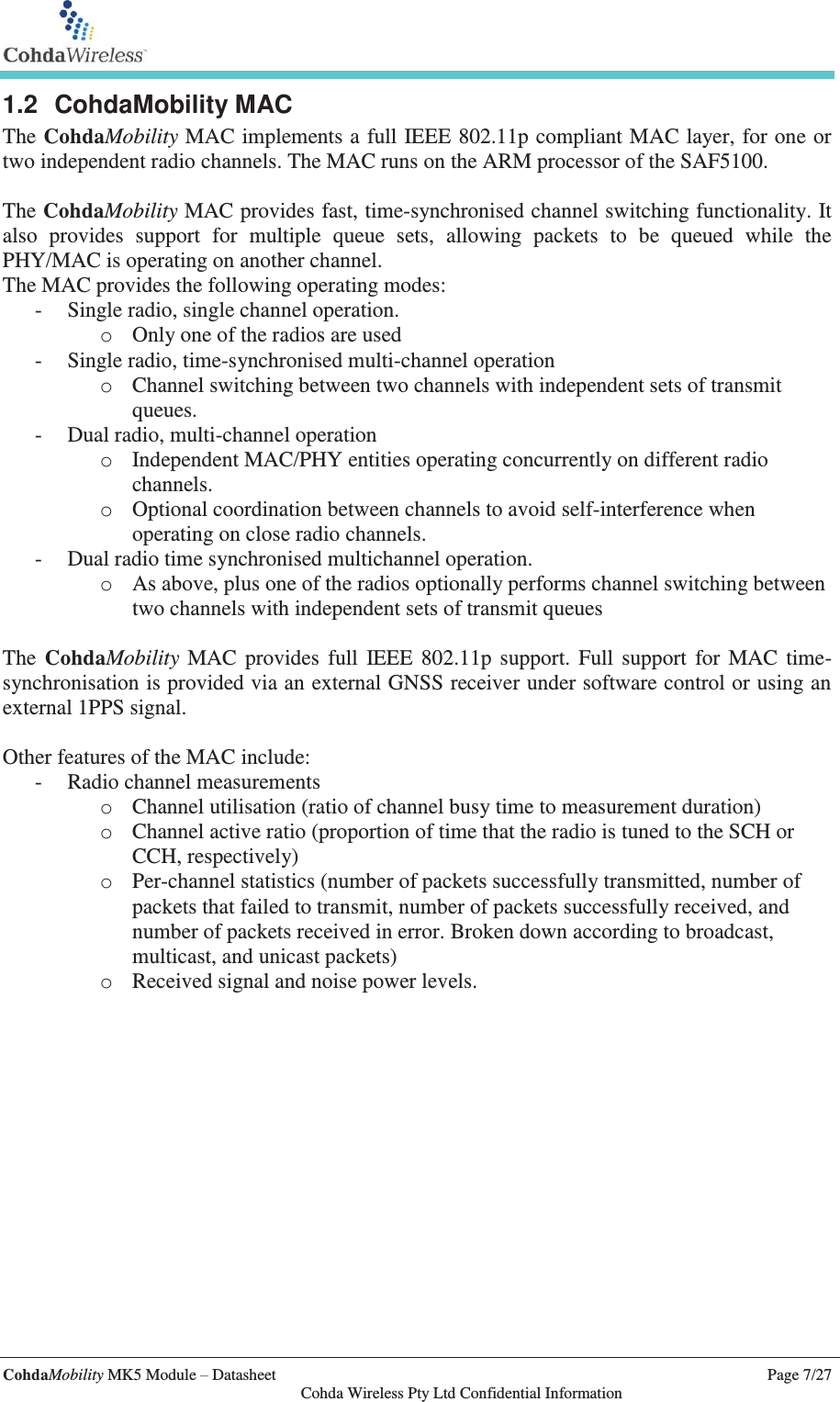
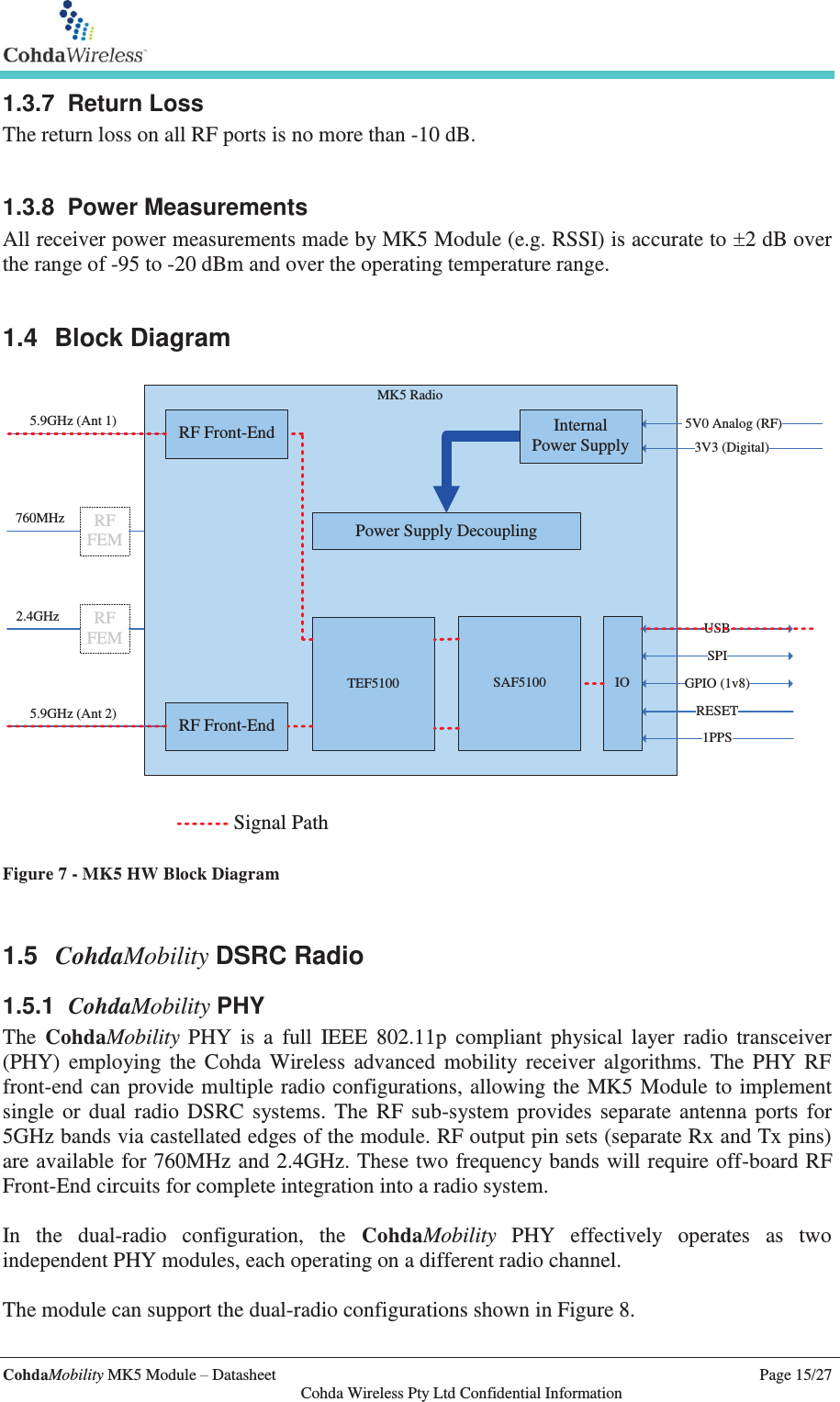
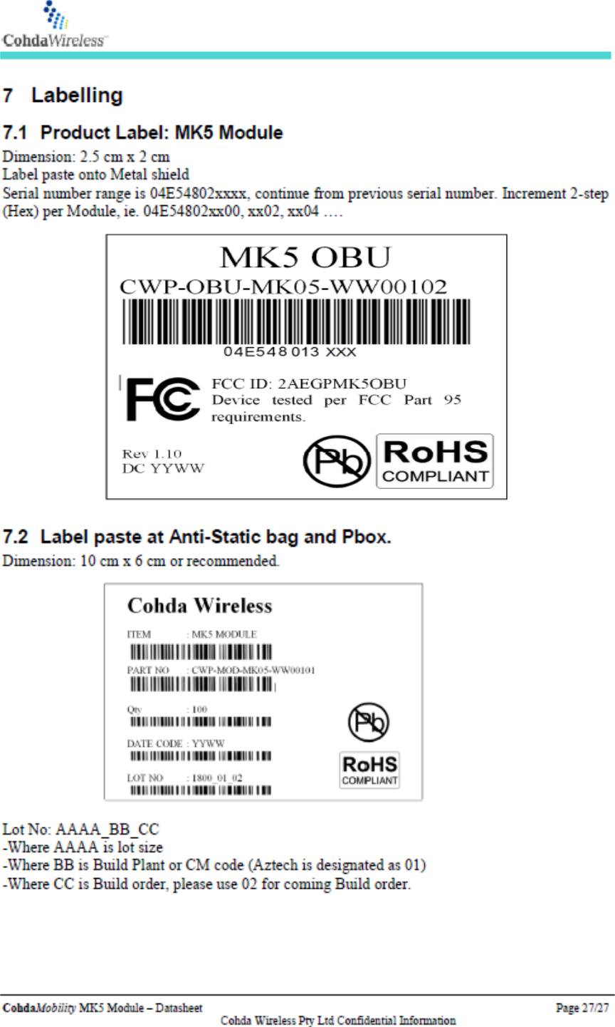
![CohdaMobility MK5 Module – Datasheet Page 8/27 Cohda Wireless Pty Ltd Confidential Information 1.3 Performance 1.3.1 Receiver Sensitivity The receive sensitivity of the MK5 Radio is presented in Table 2 for single and dual receive antennas, operating at 5.9GHz in DSRC 10MHz bandwidth mode. The packet error rate (PER) is less than 10% at a PSDU length of 1,000 octets for these input levels. The receive sensitivity is measured with a signal input directly to the antenna ports. Example plots are presented in Figure 1 and Figure 2 overleaf. Table 2 - MK5 Module Receive Sensitivity Channel No Multipath [dBm] Highway NLoS [dBm] Number of Antennas 1 Typical (Min) 2 Typical (Min) 1 Typical (Min) 2 Typical (Min) Rate ID MCS 11 1/2 BPSK -98 (-95) -99 (-97) -95 (-92) -97 (-95) 15 3/4 BPSK -96 (-93) -98 (-96) -92 (-89) -95 (-93) 10 1/2 QPSK -95 (-92) -97 (-95) -88 (-85) -92 (-90) 14 3/4 QPSK -93 (-90) -95 (-93) -86 (-83) -89 (-87) 9 1/2 16QAM -90 (-87) -92 (-90) -85 (-82) -88 (-86) 13 3/4 16QAM -86 (-83) -88 (-86) -82 (-79) -85 (-86) 8 2/3 64QAM -82 (-79) -84 (-82) na na 12 3/4 64QAM -80 (-77) -83 (-81) na na The Highway NLoS (Non Line of Sight) channel parameters used to obtain the values in Table 2 are captured in Table 3 below. Table 3 - Highway NLoS channel parameters Tap # Relative Power [dB] Delay [ns] Doppler Frequency [Hz] 0 0 0 0 1 -2 200 689 2 -5 433 -492 3 -7 700 886 This channel was used in the RF testing at the third ETSI Plugtest (CMS3). Each tap is faded using Pure Doppler, but the second antenna has a Doppler increased by 11Hz, which prevents phase synchronization of the channels. The Rx Power listed in Table 2 refers to the power of Tap 0. The values presented are typical values, measured at +25°C. The sensitivity may be reduced by approximately 1dB when operating at +85°C or -40°C.](https://usermanual.wiki/Cohda-Wireless/MK5OBU/User-Guide-2618971-Page-8.png)
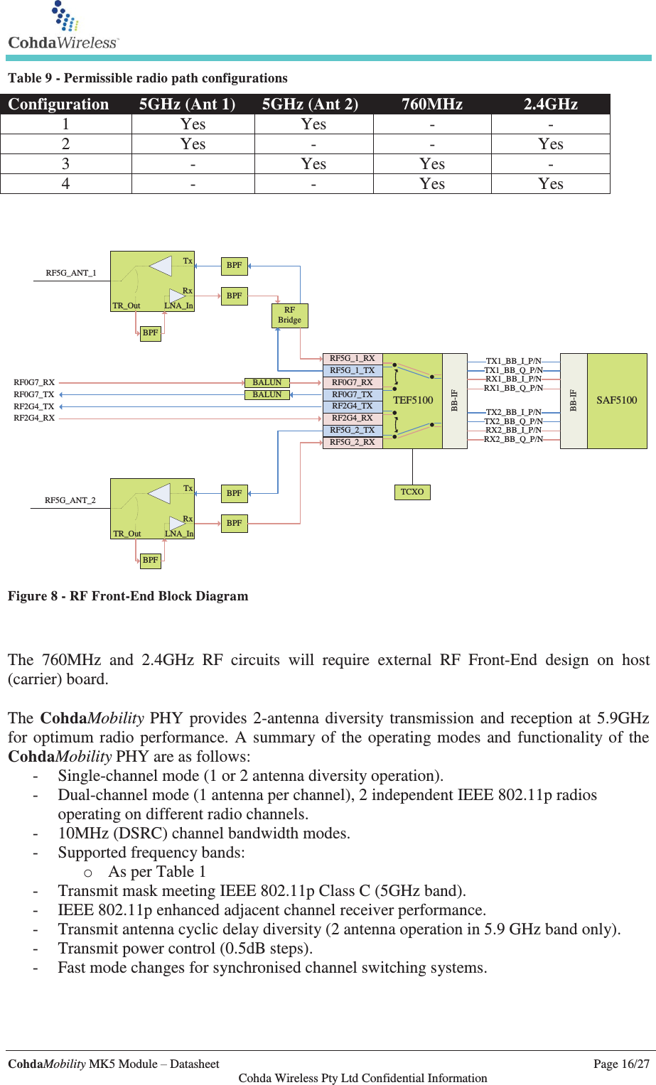
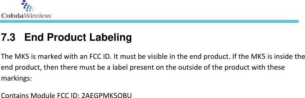
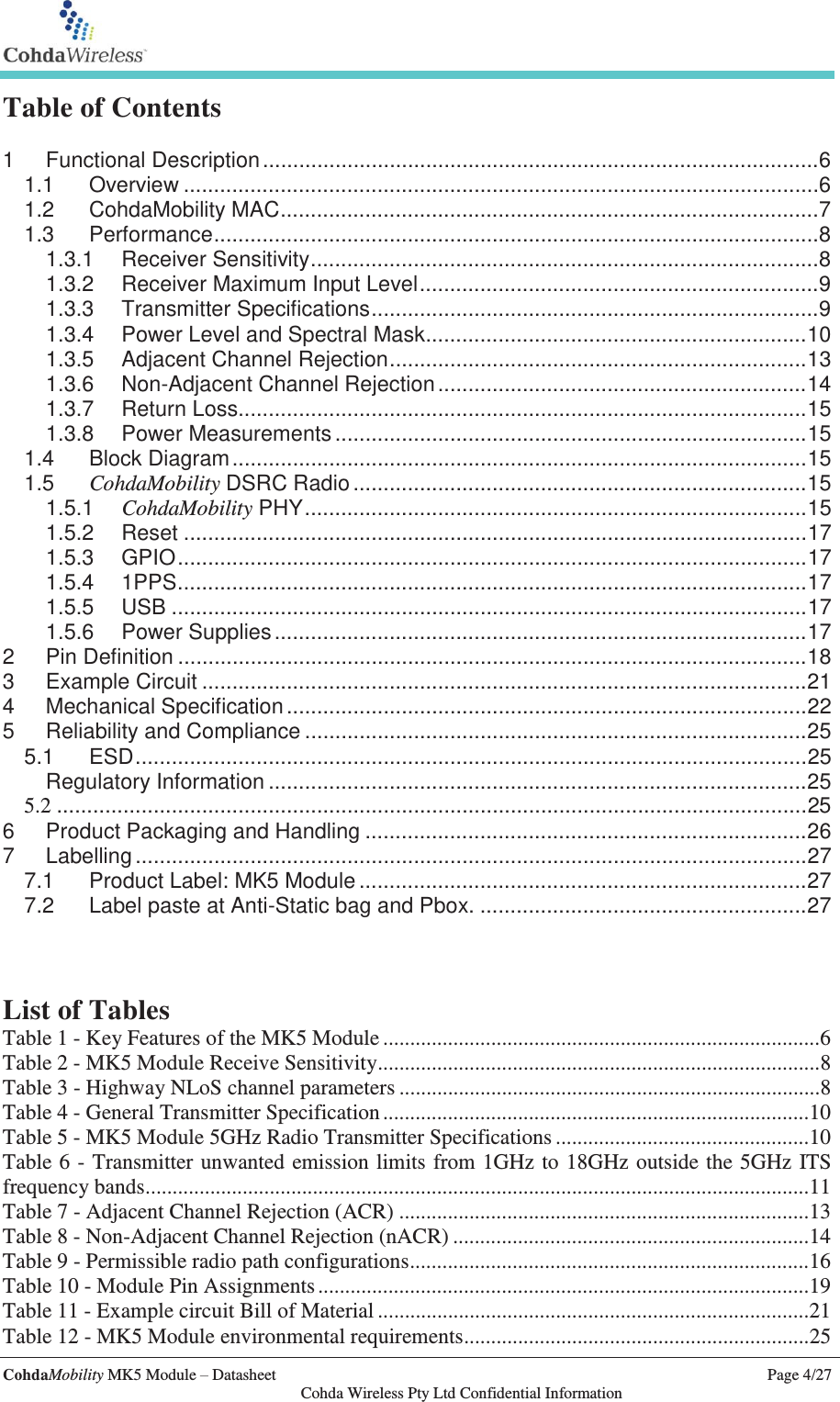
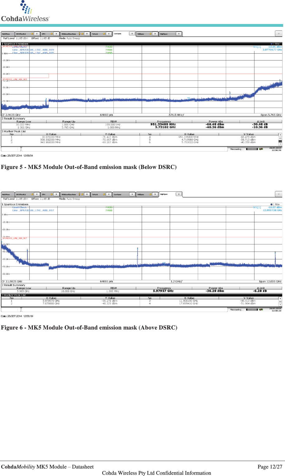
![CohdaMobility MK5 Module – Datasheet Page 10/27 Cohda Wireless Pty Ltd Confidential Information Table 4 - General Transmitter Specification Specification Performance Output centre frequency and symbol clock tolerance. ±10ppm Transmitter spectral flatness < ±2 dB in all bandwidth and modulation modes Transmitter centre frequency leakage > 15 dB below average sub-carrier power in all bandwidth and modulation modes Transmit power control step-size. 0.5 dB Transmit power control accuracy ±2 dB over temperature 1.3.4 Power Level and Spectral Mask The MK5 Module Radio maximum output power and spectral mask characteristics are outlined in Table 5. This specification applies to each of the two 5GHz antenna ports available (Ant1 and Ant2) and targets the entire temperature range. Measured results for the MK5 Module are presented in and . Figure 5 and Figure 6 presents typical Out-of-Band unwanted emission results for the MK5 Module. Table 5 - MK5 Module 5GHz Radio Transmitter Specifications Specification Performance Maximum Transmit Power +23dBm per antenna port (+26dBm effective transmit power in 2-antenna transmit mode) Minimum Transmit Power -10 dBm Transmit power control 0.5dB steps monotonically increasing/decreasing EVM per IEEE802.11-2007 (clause 17.3.9.6.3) Spectral Mask Targets DSRC class C, x 5.0 MHz, -26 dBc x 5.5 MHz, -32 dBc x 10 MHz, -40 dBc x 15 MHz, -50 dBc Out of Band Emissions Target ETSI emission mask [EN 302 571] as per Table 6 Supported channels 5GHz: 168-184](https://usermanual.wiki/Cohda-Wireless/MK5OBU/User-Guide-2618971-Page-10.png)
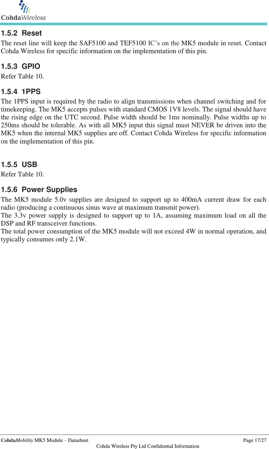
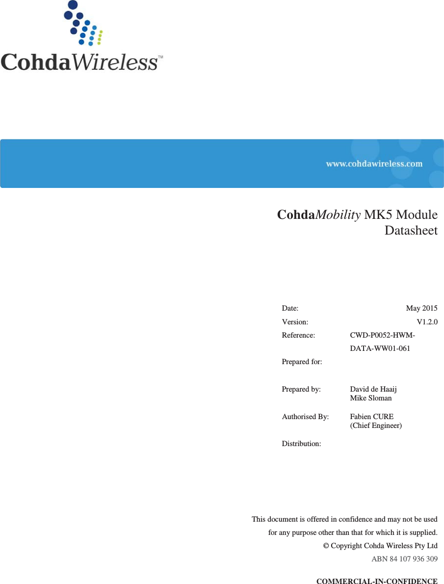
![CohdaMobility MK5 Module – Datasheet Page 11/27 Cohda Wireless Pty Ltd Confidential Information Table 6 - Transmitter unwanted emission limits from 1GHz to 18GHz outside the 5GHz ITS frequency bands Frequency Range Res BW [MHz] Maximum Power (EIRP) [dBm] 1 GHz < f < 5,795 GHz 1 -30 5,795 GHz < f < 5,815 GHz 1 -40 5,815 GHz < f < 5,850 GHz 1 -40 5,850 GHz < f < 5,855 GHz 1 -30 5,925 GHz < f < 5,965 GHz 1 -40 5,965 GHz < f < 18 GHz 1 -30 Figure 3 - MK5 Module Class-C Transmission Mask Figure 4 - MK5 Module EVM and Transmit Power](https://usermanual.wiki/Cohda-Wireless/MK5OBU/User-Guide-2618971-Page-11.png)
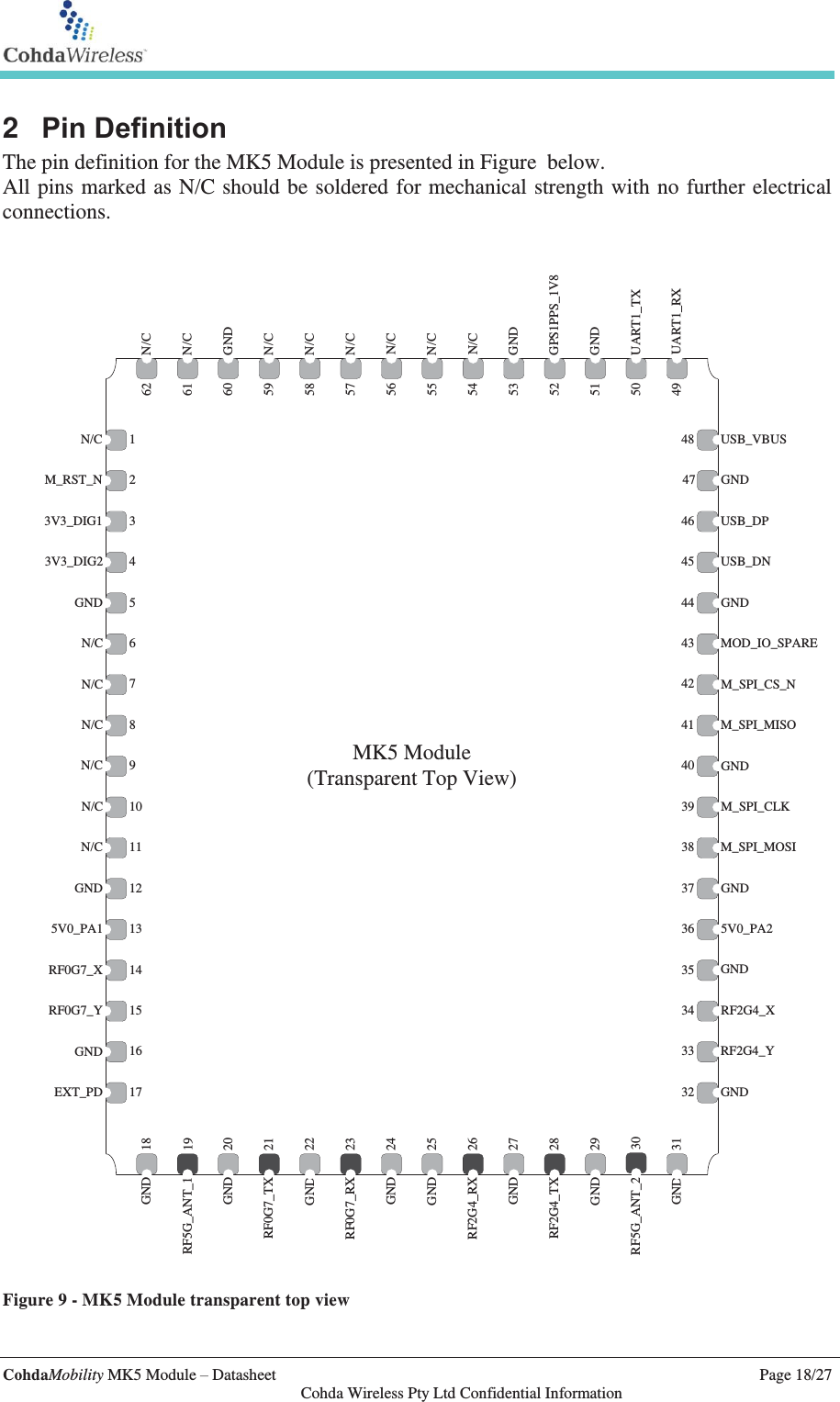
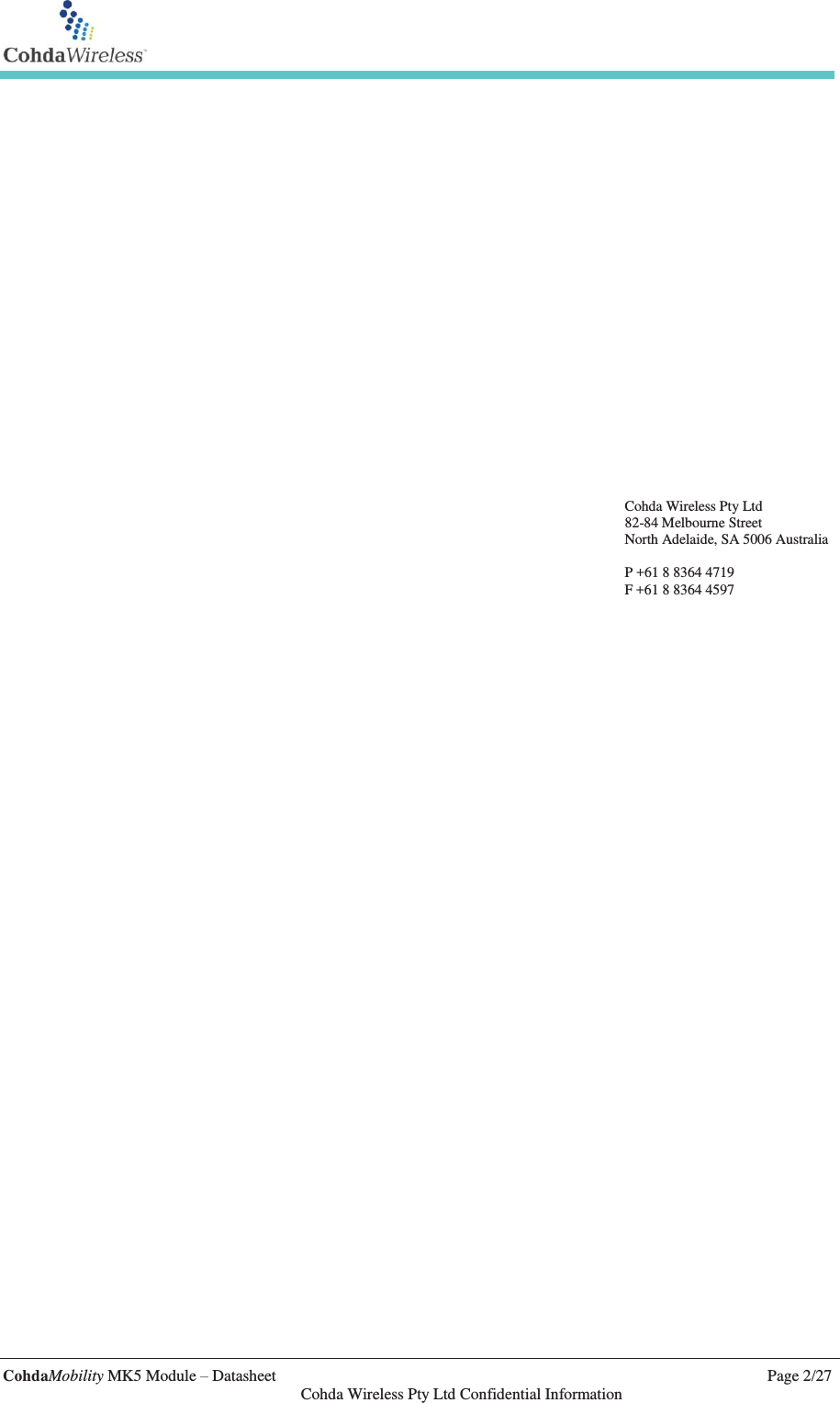
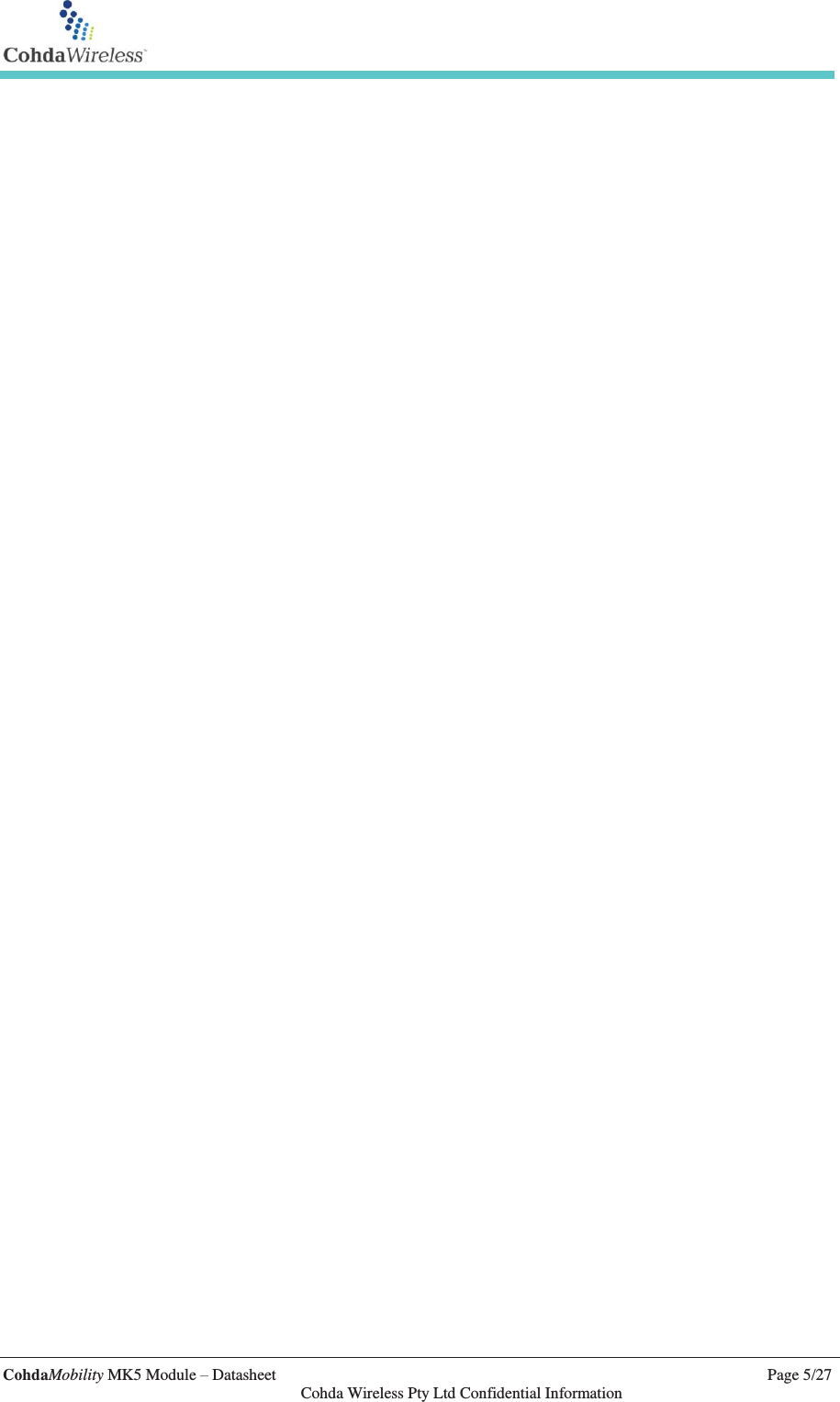
![CohdaMobility MK5 Module – Datasheet Page 13/27 Cohda Wireless Pty Ltd Confidential Information 1.3.5 Adjacent Channel Rejection The adjacent channel rejection of a MK5 Module is measured by setting the desired signal strength 3 dB above the receive sensitivity specified in Table 18-14 of the IEEE802.11-2012 standardTable 2 and raising the power of the interfering signal until 10% PER is caused for a PSDU length of 1000 octets. The power difference between the interfering and the desired channel is the corresponding adjacent channel rejection. The interfering signal in the adjacent channel is a conformant OFDM signal, meeting the DSRC Class C mask, unsynchronized with the signal in the channel under test. The receive sensitivity values are measured with a signal input directly to the Antenna Ports. Measured results for the MK5 Module adjacent channel rejection, together with the target nACR values obtained from the IEEE802.11-2012 standard, are provided in Table 7 Table 7 - Adjacent Channel Rejection (ACR) Modulation Target ACR [dB] Target opt. enh. ACR [dB] MK5 Typical ACR [dB] ½ BPSK 16 28 37 ¾ BPSK 15 27 33 ½ QPSK 13 25 35 ¾ QPSK 11 23 29 ½ 16QAM 8 20 29 ¾ 16QAM 4 16 25 ⅔ 64QAM 0 12 22 ¾ 64QAM -1 11 20](https://usermanual.wiki/Cohda-Wireless/MK5OBU/User-Guide-2618971-Page-13.png)
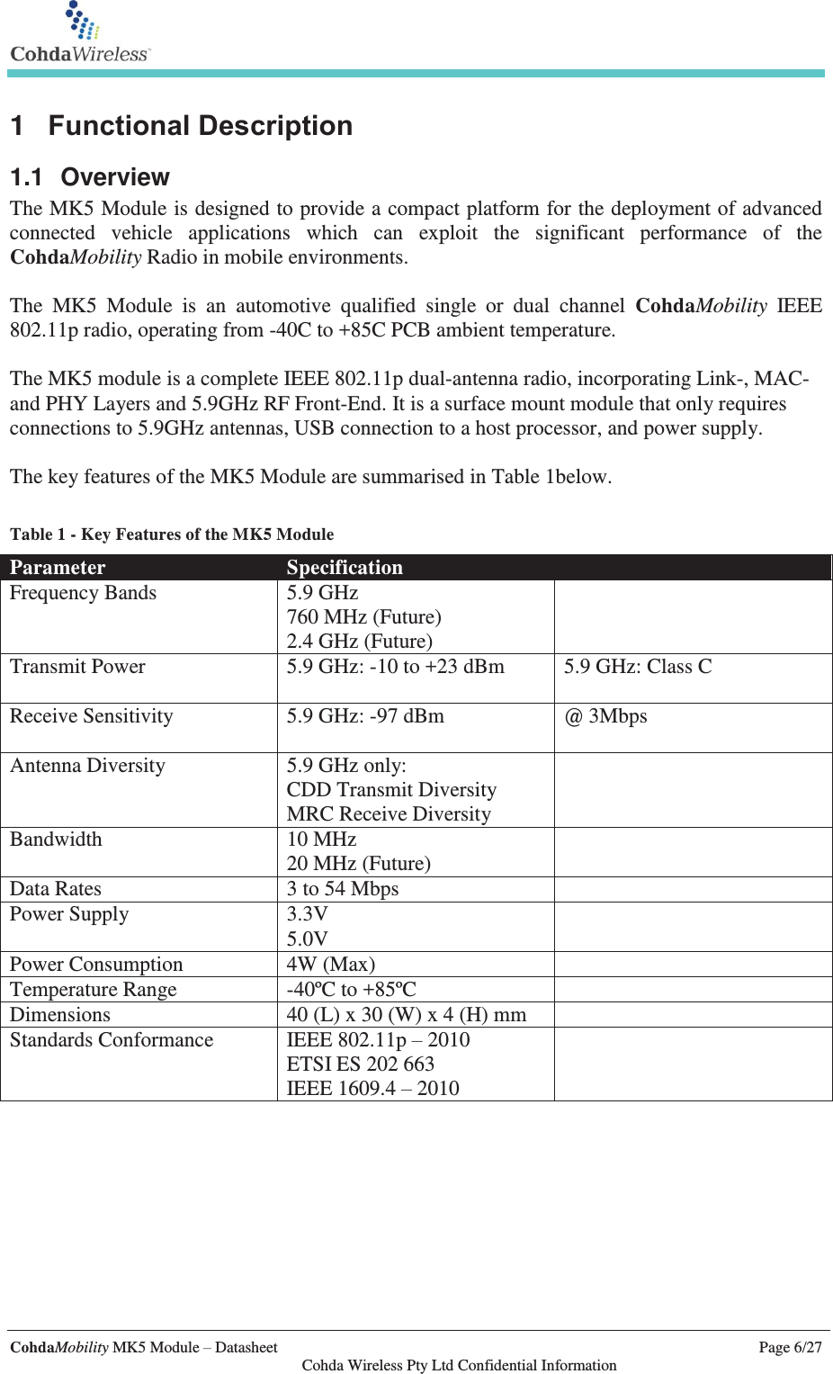
![CohdaMobility MK5 Module – Datasheet Page 14/27 Cohda Wireless Pty Ltd Confidential Information 1.3.6 Non-Adjacent Channel Rejection The non-adjacent channel rejection of a MK5 Module Radio is measured by setting the desired signal’s strength 3 dB above the rate-dependent sensitivity specified in Table 18-14 of the IEEE802.11-2012, and raising the power of the interfering signal until a 10% PER occurs for a PSDU length of 1000 octets. The power difference between the interfering and the desired channel is the corresponding nonadjacent channel rejection. The interfering signal in the non-adjacent channel is a conformant OFDM signal, targeting the DSRC Class C mask, unsynchronized with the signal in the channel under test. The receive sensitivity values are measured with a signal input directly to the Antenna Ports. Measured results for the MK5 Module non-adjacent channel rejection, together with the target nACR values obtained from the IEEE802.11-2012 standard, are provided in Table 8. Table 8 - Non-Adjacent Channel Rejection (nACR) Modulation Target nACR [dB] Target opt. enh. nACR [dB] Typical nACR [dB] ½ BPSK 32 42 51 ¾ BPSK 31 41 48 ½ QPSK 29 39 48 ¾ QPSK 27 37 45 ½ 16QAM 24 34 42 ¾ 16QAM 20 30 38 ⅔ 64QAM 16 26 34 ¾ 64QAM 15 25 32](https://usermanual.wiki/Cohda-Wireless/MK5OBU/User-Guide-2618971-Page-14.png)