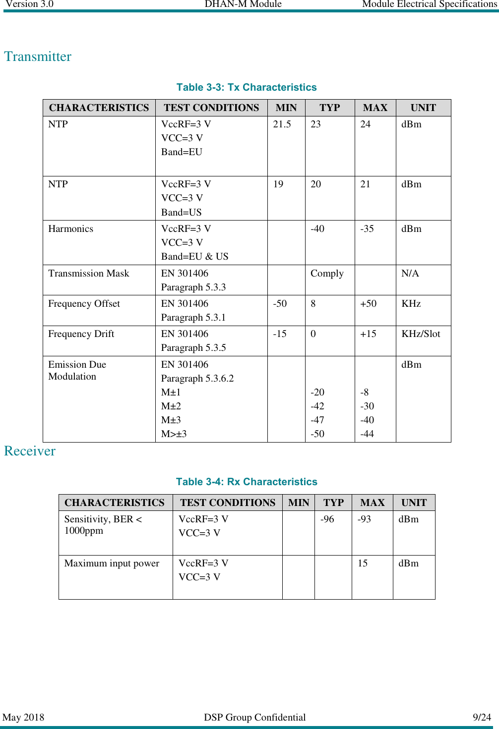
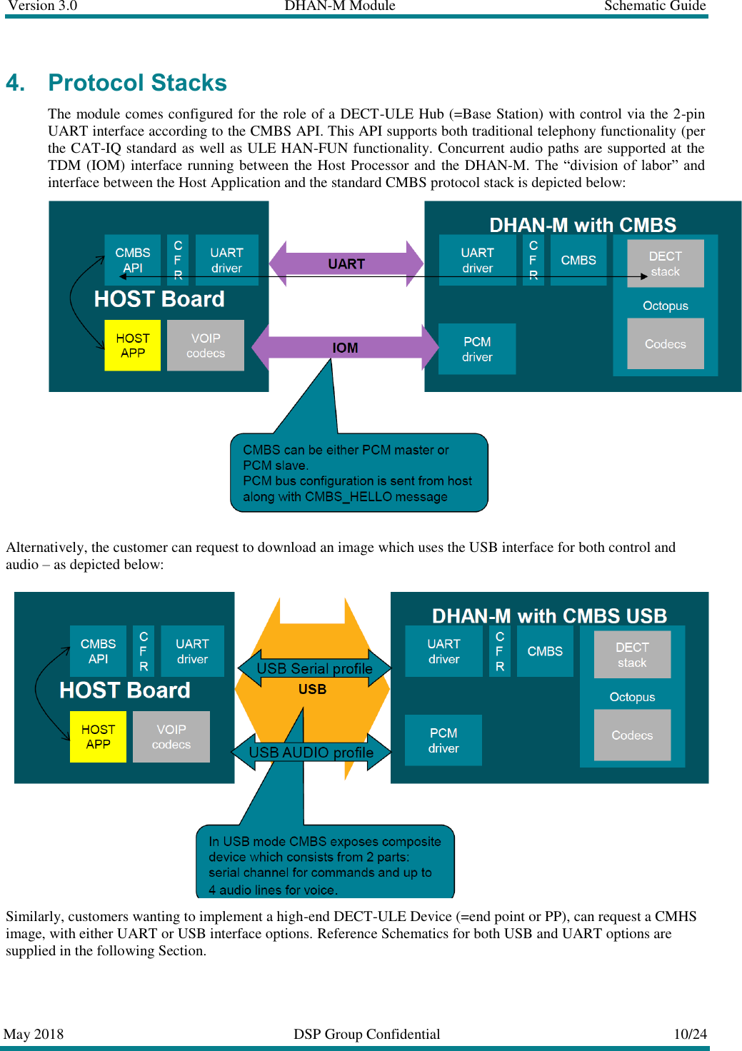
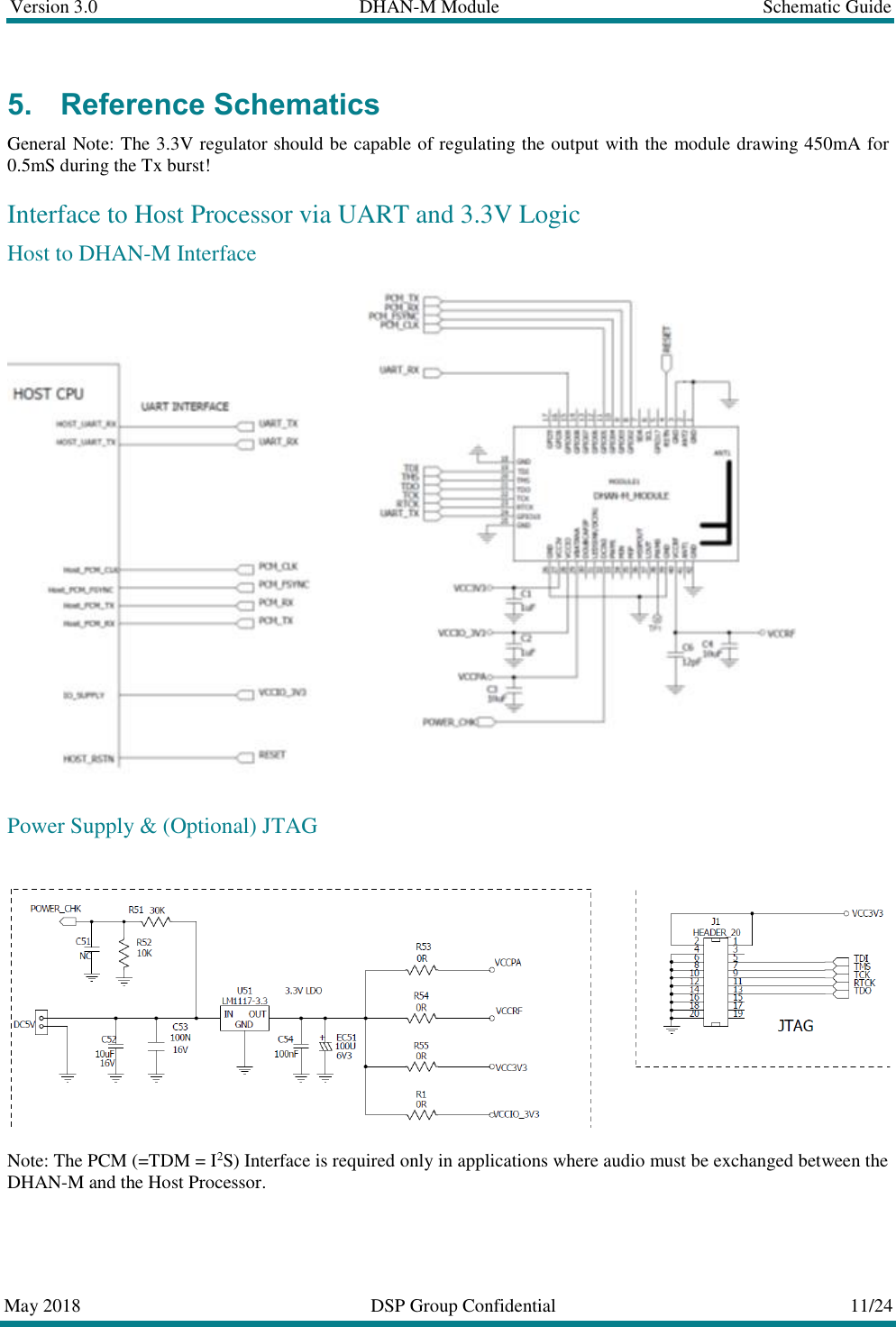
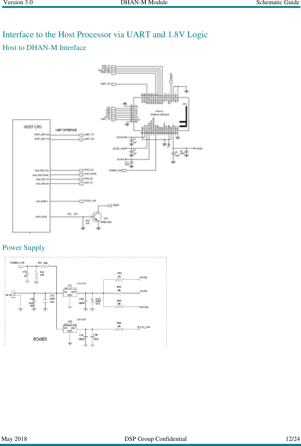
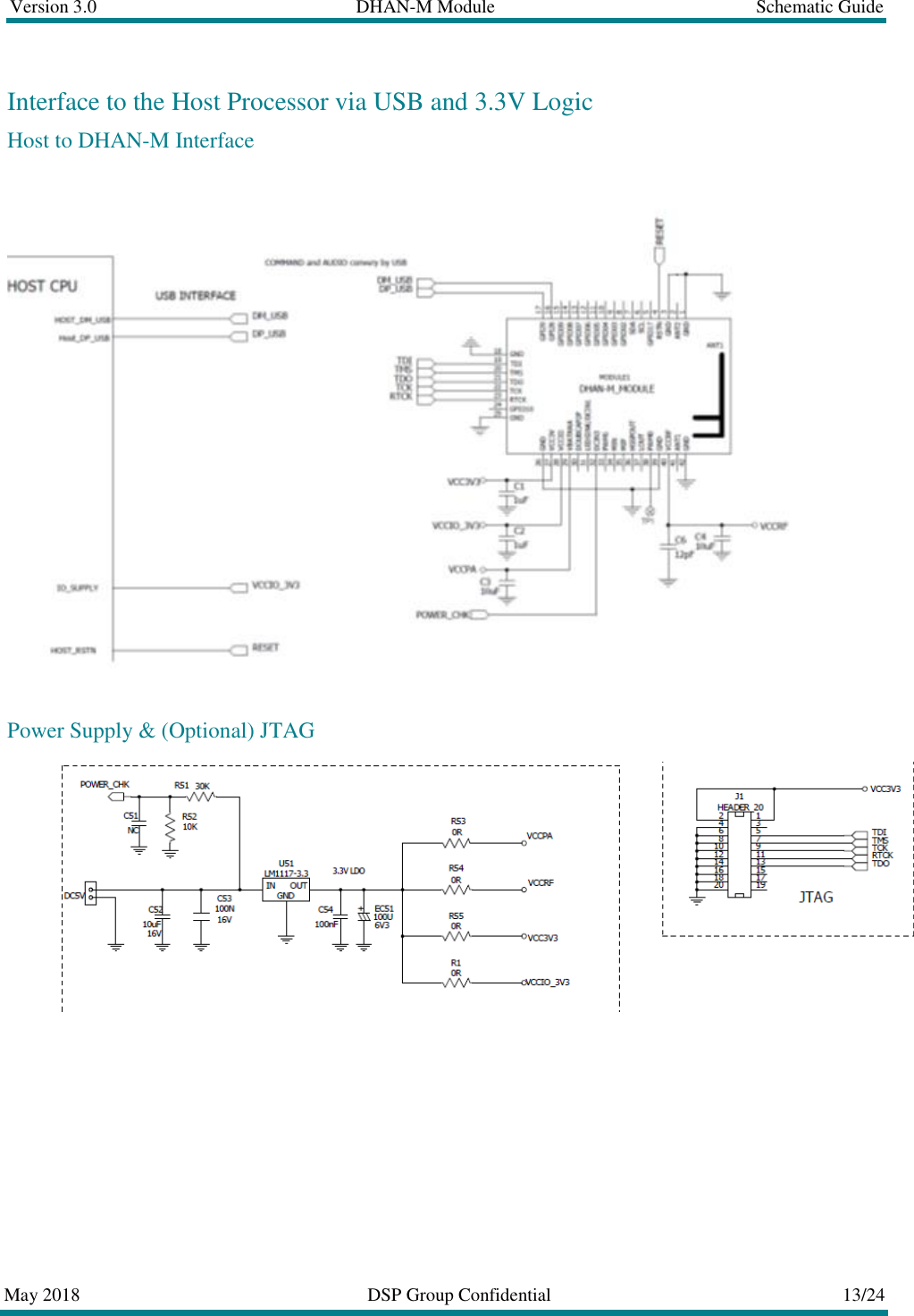
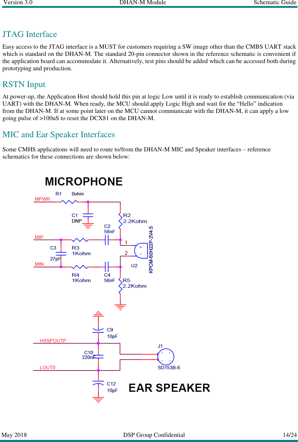
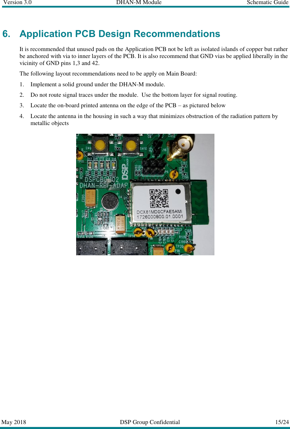
DSP Group DHANM DECT Module User Manual DHX91 DHAN Module Datasheet

DSP Group Ltd DECT Module DHX91 DHAN Module Datasheet

Users Manual

  DHAN-M Module DECT-ULE Platform   Datasheet Version: 3.0 May 29, 2018
Version 3.0  DHAN-M Module  Worldwide Sites       May 2018  DSP Group Confidential  2/24   Headquarters  USA  DSP Group Inc. 161 S San Antonio Rd Suite 10 Los Altos, CA 94022 Tel: (408)986-4300  Fax:(408)986-4323  Israel DSP Group Ltd. 5 Shenkar Street Herzelia, Israel 4672505 Tel: 972-9-952-9696  Fax: 972-9-954-1234     Europe  Germany DSPG Technologies GmbH Nelson-Mandela-Platz 18  90459 Nurnberg  Tel: +49-911-2001-0 Fax: +49-911-2001-1210  Scotland DSPG Edinburgh Ltd. Geddes House Kirkton North  Livingston EH54 6GU Tel: +44-1223-772200      APAC  China DSP Group (HK) Limited Unit 1-4, 11/F, 909 Cheung Sha Wan Rd. Kowloon  Hong Kong  Tel: +852-(3965)-5888   DSP Group (Shenzhen) Limited Room 1819, 18/F Kerry Centre, Renminnan Road, Shenzhen, China 518001 Tel: +(86 755) 2518 1214  Ascend Technology Inc. Room 1303,  New World Center,  No.6009 Yitian Road,  Futian District, Shenzhen City, China Tel: +86-755-820-24598 Fax: +86-755-239-82986  Ascend Technology Inc. Rm 607,  Hui Huang International Center, 1st Place, Shangdi 10th Road, Haidian District, Beijing City, P.R.  Japan DSP Group (Japan) Inc. 1-29-1 Nishi-Gotanda Shinagawa-Ku Tokyo 141-0031  Tel:+81-(3)-3493-3050   Tomen Electronics  8-27, Kohnan 1 Chome, Minato-ku, Tokyo  108-8510, Japan  Tel: +81-(3)-5462-9619  Fax: +81-(3)-5462-9686   Korea Daesung Semiconductors  140-848, RM 401 Wonhyo BD. 46-1 Wonhyo-ro 3ka, Yongsan-gu, Seoul, Korea  Tel: +82-(2)-3272-7300 Fax: +82-(2)-712-4632-3  India DSP Technology Indian Private Limited Information Technology Park Nagawara Village Kasaba Hobli Bangalore 560045  Tel: +91 80 4024 8399  Taiwan Ascendtek Electronics, Inc 11F-7, No. 77, Sec. 1 Hsin Tai Wu Rd.,  Hsi Chih Taipei Hsien, Taiwan, R.O.C Tel: 886-2-2698-8696  Fax: 886-2-8698-2138           This document is provided by DSP Group, Inc. and/or one or more of its subsidiaries (“DSP Group”). All information and data contained in this document is for informational purposes only, without any commitment on the part of DSP Group, and is not to be considered as an offer for a contract. DSP Group shall not be liable, in any event, for any claims for damages or any other remedy in any jurisdiction whatsoever, whether in an action in contract, tort (including negligence and strict liability) or any other theory of liability, whether in law or equity including, without limitation, claims for damages or any other remedy in whatever jurisdiction, and shall not assume responsibility for patent infringements or other rights to third parties, arising out of or in connection with this document. Further, DSP Group reserves the right to revise this publication and to make changes to its content, at any time, without obligation to notify any person or entity of such revision changes. These materials are copyrighted and any unauthorized use of these materials may violate copyright, trademark, and other laws. Therefore, no part of this publication may be reproduced, photocopied, stored on a retrieval system, or transmitted without the express written consent of DSP Group. Any new issue of this document invalidates previous issues. DSP Group reserves the right to revise this publication and to make changes to its content, at any time, without obligation to notify any person or entity of such revision changes. © 2018 DSP Group Confidential. All rights reserved.
Version 3.0  DHAN-M Module  Table of Contents  May, 2018  DSP Group Confidential  3/24  TABLE OF CONTENTS 1. INTRODUCTION ........................................................................................................................................... 5 General Description ............................................................................................................................................ 5 Features ............................................................................................................................................................... 5 Block Diagram .................................................................................................................................................... 5 2. PIN AND SIGNAL DESCRIPTION ............................................................................................................... 6 3. MODULE ELECTRICAL SPECIFICATIONS .............................................................................................. 8 Absolute Maximum Rating ................................................................................................................................. 8 Recommended Operating Conditions ................................................................................................................. 8 Peak Currents and Hibernation Current .............................................................................................................. 8 Transmitter .......................................................................................................................................................... 9 Receiver .............................................................................................................................................................. 9 4. PROTOCOL STACKS .................................................................................................................................. 10 5. REFERENCE SCHEMATICS ...................................................................................................................... 11 Interface to Host Processor via UART and 3.3V Logic .................................................................................... 11 Host to DHAN-M Interface ........................................................................................................................ 11 Power Supply & (Optional) JTAG ............................................................................................................. 11 Interface to the Host Processor via UART and 1.8V Logic .............................................................................. 12 Host to DHAN-M Interface ........................................................................................................................ 12 Power Supply ............................................................................................................................................. 12 Interface to the Host Processor via USB and 3.3V Logic ................................................................................. 13 Host to DHAN-M Interface ........................................................................................................................ 13 Power Supply & (Optional) JTAG ............................................................................................................. 13 JTAG Interface ................................................................................................................................................. 14 RSTN Input ....................................................................................................................................................... 14 MIC and Ear Speaker Interfaces ....................................................................................................................... 14 6. APPLICATION PCB DESIGN RECOMMENDATIONS ............................................................................ 15 7. DIVERSITY ANTENNA (OPTION) ............................................................................................................ 16 8. ASSEMBLY INFORMATION ..................................................................................................................... 17 Mechanical Drawing ......................................................................................................................................... 17 PCB Metal Land Pattern Recommendation ...................................................................................................... 18 PCB Solder Mask Recommendation ................................................................................................................. 19 PCB Stencil Pattern Recommendation .............................................................................................................. 20 Pick & Place, Reflow ........................................................................................................................................ 20 9. SUPPLEMENTARY INFORMATION ........................................................................................................ 21 Labeling (appended to the module shield) ........................................................................................................ 21 RF Exposure information and statement ........................................................................................................... 21 FCC & IC Interference statement RFPI and EMC .................................................................................................................................................. 22 (DoC) Declaration of conformity OEM Notes IC labeling requirements for the final end product Ordering Information ........................................................................................................................................ 23
Version 1.5  DHX91 DHAN Module Datasheet  Table of Contents       May 2018  DSP Group Confidential  4/24   Change Log ....................................................................................................................................................... 24
Version 3.0  DHAN-M Module  Introduction       May 2018  DSP Group Confidential  5/24   1. Introduction General Description The DSPG DHAN-M module is based on the state-of-the-art DCX81 - a 2nd generation DECT SOC. The DHAN-M module is suited for DECT-ULE applications that employ a processor external to the DHAN-M. The DHAN-M can serve as a DECT-ULE Hub (=Base Station) when loaded with a CMBS SW image. This image includes standard DECT-ULE MAC-PHY connectivity as well as CAT-IQ functionality for traditional DECT telephony and HAN-FUN (ie the ULE Alliance Standard) functionality for ULE (low-power packet mode).  The DHAN-M can also be loaded with a SW image that that empowers the module with a DECT “handset” profile (CMHS). As above, both UART and USB interfaces are available for control and, in the case where audio needs to be transferred between the CMHS target and the Host Processor, TDM or USB Audio Class can be utilized.  In either case, the DHAN-M interfaces with the Host Processor via UART or USB. Audio is transferred either via TDM (with control via UART) or via USB (Audio Class). Features  Excellent radio performance, with over 123dB system gain  A printed antenna is included in the module. A 2nd antenna port is provided and can be routed to an optional diversity antenna located elsewhere in the application housing  Radio covers all regional DECT bands. A simple re-configuration of the EEPROM is required  Radio is fully compliant with ETSI DECT and ULE standards. Regulatory (EU, FCC) certification is pending  Compact module footprint of 27.2x15.2x3.3 (including the RF shield height)  Operating Temperature spanning -40ºC to 85ºC Block Diagram  DHAN-M Module Block Diagram
Version 3.0   DHAN-M Module  Pin and Signal Description  May 2018  DSP Group Confidential  6/24  2. Pin and Signal Description  PIN NO.  NAME  DESCRIPTION/TYPE 1  GND  Place many vias in the vicinity of this pin 2  ANT2  Optional port for connection to a diversity antenna located elsewhere in the housing. Otherwise terminate with a 51-Ohm resistor 3  GND  Place many vias in the vicinity of this pin 4  RSTN  Resets the DCX81 SOC. See reference schematic and comments 5  GPIO17   6  SCL (GPIO0)  GPIO or I2C Clock. Open Drain, reset value is floating 7  SDA (GPIO1)  GPIO or I2C Data. Open Drain, reset value is floating 8  GPIO2 (PCM_Tx)  TDM Tx Data 9  GPIO3 (PCM_Rx)  TDM_Rx Data 10 GPIO4 (PCM_FSYNC)  TDM Frame Sync 11 GPIO5 (PCM_CLK)  TDM SCLK 12 GPIO6 (SPI_MOSI)  SPI Data Input to the DHAN-M 13 GPIO7 (SPI_MISO)  SPI Data Output from the DHAN-M 14  GPIO8 (SPI_CLK)  SPI Clock 15 GPIO9 (RxD or SPI_CS)  UART Rx (most typically) or SPI Chip Select 16 GPIO28 (DM_USB)  USB Positive Pin 17  GPIO29 (DP_USB)  USB Negative Pin 18 GND   19  TDI  JTAG Data In. Should be connected to TP 20  TMS  JTAG Mode Select. Should be connected to TP 21  TDO  JTAG Data Out. Should be connected to TP 22  TCK  JTAG Clock. Should be connected to TP  23  RTCK  JTAG Reset. Should be connected to TP 24  GPIO10 (TxD)  GPIO or UART Tx 25 GND   26 GND
Version 3.0   DHAN-M Module  Pin and Signal Description  May 2018  DSP Group Confidential  7/24  PIN NO.  NAME  DESCRIPTION/TYPE 27  VCC3V  Power Supply Input 28  VCCIO  Powers the IO level shifters. 1.8 or 3.3V. See reference schematics 29  VBATANA  Power Supply Input for the analog portion of the SOC 30  DOUBCAP2P   31 LEDSINK/DCIN1   32  DCIN3  ADC. Check of Power. See reference schematic 33  PWM1   34  MIN  Microphone negative input 35  MIP  Microphone positive input 36  HSSPOT  Handset/Headset positive speaker output 37  LOUT  Line Output or Handset/Headset negative speaker output 38  PWM0   39 GND   40 VccRF Power Supply Input to RF. Add 10pF bypass capacitor adjacent to this pin! 41  ANT1  Test pin. Leave unconnected 42 GND  Place many vias in the vicinity of this pin
Version 3.0  DHAN-M Module  Module Electrical Specifications  May 2018  DSP Group Confidential  8/24  3. Module Electrical Specifications All parameters are for 25ºC. Absolute Maximum Rating Table 3-1: Absolute Maximum Rating Minimum Voltage Applied to all pins: -0.3V Maximum Voltage Applied to all pins: +4.6V Storage Temperature Range: -45 to 90ºC Note: Functionality at or above these limits is not implied. Exposure to absolute maximum ratings for extended periods may affect device reliability. Recommended Operating Conditions Table 3-2: Recommended Operating Conditions RATING   CONDITIONS  MIN  TYP  MAX  UNIT Operating ambient temperature   -40  +25  +85  °C VccRF, VCC    2  3.0  3.6  V JTAG, UART  VIL VIH VOL VOH (VCC is at nominal 3V)   2.0  2.4  0.8  0.4 V DCIN3    2  3.0  VCC  V  Peak Currents and Hibernation Current  PARAMETER  TEST CONDITIONS  TYP  MAX  UNIT Tx Current  VccRF=3 V VCC=3 V Band=EU @ 23dBm 400 480 mA Tx Current  VccRF=3 V VCC=3 V Band=US @ 21 dBm 250 300 mA Rx Current  VccRF=3 V VCC=3 V  125 135 mA
Version 3.0  DHAN-M Module  Module Electrical Specifications  May 2018  DSP Group Confidential  9/24  Transmitter Table 3-3: Tx Characteristics CHARACTERISTICS   TEST CONDITIONS  MIN  TYP  MAX  UNIT NTP  VccRF=3 V VCC=3 V Band=EU 21.5  23 24  dBm NTP  VccRF=3 V VCC=3 V Band=US  19 20 21  dBm Harmonics   VccRF=3 V VCC=3 V Band=EU & US   -40  -35  dBm Transmission Mask  EN 301406 Paragraph 5.3.3   Comply    N/A Frequency Offset  EN 301406 Paragraph 5.3.1 -50  8  +50  KHz Frequency Drift  EN 301406 Paragraph 5.3.5 -15  0  +15  KHz/Slot Emission Due Modulation  EN 301406 Paragraph 5.3.6.2 M±1 M±2 M±3 M>±3     -20 -42 -47 -50   -8 -30 -40 -44 dBm Receiver Table 3-4: Rx Characteristics CHARACTERISTICS   TEST CONDITIONS  MIN  TYP  MAX  UNIT Sensitivity, BER < 1000ppm  VccRF=3 V VCC=3 V    -96  -93  dBm Maximum input power  VccRF=3 V VCC=3 V      15  dBm
Version 3.0  DHAN-M Module  Schematic Guide  May 2018  DSP Group Confidential  10/24  4. Protocol Stacks The module comes configured for the role of a DECT-ULE Hub (=Base Station) with control via the 2-pin UART interface according to the CMBS API. This API supports both traditional telephony functionality (per the CAT-IQ standard as well as ULE HAN-FUN functionality. Concurrent audio paths are supported at the TDM (IOM) interface running between the Host Processor and  the DHAN-M. The “division of labor”  and interface between the Host Application and the standard CMBS protocol stack is depicted below:   Alternatively, the customer can request to download an image which uses the USB interface for both control and audio – as depicted below:  Similarly, customers wanting to implement a high-end DECT-ULE Device (=end point or PP), can request a CMHS image, with either UART or USB interface options. Reference Schematics for both USB and UART options are supplied in the following Section.
Version 3.0  DHAN-M Module  Schematic Guide  May 2018  DSP Group Confidential  11/24  5. Reference Schematics General Note: The 3.3V regulator should be capable of regulating the output with the module drawing 450mA for 0.5mS during the Tx burst! Interface to Host Processor via UART and 3.3V Logic Host to DHAN-M Interface  Power Supply & (Optional) JTAG   Note: The PCM (=TDM = I2S) Interface is required only in applications where audio must be exchanged between the DHAN-M and the Host Processor.
Version 3.0  DHAN-M Module  Schematic Guide  May 2018  DSP Group Confidential  12/24  Interface to the Host Processor via UART and 1.8V Logic Host to DHAN-M Interface  Power Supply
Version 3.0  DHAN-M Module  Schematic Guide  May 2018  DSP Group Confidential  13/24  Interface to the Host Processor via USB and 3.3V Logic Host to DHAN-M Interface  Power Supply & (Optional) JTAG
Version 3.0  DHAN-M Module  Schematic Guide  May 2018  DSP Group Confidential  14/24  JTAG Interface Easy access to the JTAG interface is a MUST for customers requiring a SW image other than the CMBS UART stack which is standard on the DHAN-M. The standard 20-pin connector shown in the reference schematic is convenient if the application board can accommodate it. Alternatively, test pins should be added which can be accessed both during prototyping and production. RSTN Input At power-up, the Application Host should hold this pin at logic Low until it is ready to establish communication (via UART) with the DHAN-M. When ready, the MCU should apply Logic High and wait for the “Hello” indication from the DHAN-M. If at some point later on the MCU cannot communicate with the DHAN-M, it can apply a low going pulse of >100uS to reset the DCX81 on the DHAN-M. MIC and Ear Speaker Interfaces Some CMHS applications will need to route to/from the DHAN-M MIC and Speaker interfaces – reference schematics for these connections are shown below:
Version 3.0  DHAN-M Module  Schematic Guide  May 2018  DSP Group Confidential  15/24  6. Application PCB Design Recommendations It is recommended that unused pads on the Application PCB not be left as isolated islands of copper but rather be anchored with via to inner layers of the PCB. It is also recommend that GND vias be applied liberally in the vicinity of GND pins 1,3 and 42. The following layout recommendations need to be apply on Main Board:  1. Implement a solid ground under the DHAN-M module. 2. Do not route signal traces under the module.  Use the bottom layer for signal routing. 3. Locate the on-board printed antenna on the edge of the PCB – as pictured below 4. Locate the antenna in the housing in such a way that minimizes obstruction of the radiation pattern by metallic objects
Version 3.0  DHAN-M Module  Schematic Guide  May 2018  DSP Group Confidential  16/24  7. Diversity Antenna (OPTION) If no diversity antenna is planned, a 51-Ohm chip resistor should be placed as close as possible from Pin2 to GND. Alternatively, Pin2 can be routed to a Diversity antenna. There are several options for a diversity antenna: a) Route a 50-ohm line to an RF connector on the Application Board and RF cable to a connectorized commercial antenna mounted in elsewhere in the device housing b) Route the 50-ohm line to the antenna feed point located ~8cm from the on-board antenna feed-point. This antenna can be a ¼ wave monopole wire antenna, chip or printed antenna (similar to the on-board antenna). Guidelines for such antennas are given below:  A wire antenna can be inserted through a via at the feed-point. It should extend vertically with respect to the face of the PCB. The total length of the wire antenna should be ¼ Lambda (~40.0 mm). It is important to ensure an adequate ground plane near the feed point in order to obtain maximal antenna gain and efficiency  Off the shelf chip antennas: P/N  Manufacturer H2U74W1H1M0100  Unictron ANT8868LL00R1880A  Yageo CAN4311112001881K  Yageo W3022  Pulse Elect  Inverted-F printed antenna – See www.dspg.com for analysis and database for such an antenna. In this case, the orientation of the antenna should be rotated 90⁰ with respect to the DHAN-M antenna
Version 3.0  DHAN-M Module  Schematic Guide  May 2018  DSP Group Confidential  17/24  8. Assembly Information An electronic version of the information in this Section can be downloaded from the DSP Group website, in the HW Developer's Collateral section. The files Mechanical Drawing
Version 3.0  DHAN-M Module  Schematic Guide  May 2018  DSP Group Confidential  18/24  PCB Metal Land Pattern Recommendation
Version 3.0  DHAN-M Module  Schematic Guide  May 2018  DSP Group Confidential  19/24  PCB Solder Mask Recommendation
Version 3.0  DHAN-M Module  Schematic Guide  May 2018  DSP Group Confidential  20/24  PCB Stencil Pattern Recommendation  Pick & Place, Reflow The DHAN-M module uses a flat shield cover to facilitate a fully automatic assembly process.  For backing and  reflow  recommendations,  use  MSL  3  in  the  JEDEC/IPC  standard  J-STD-20b.  The  temperature classification (TC) for the module is 245° C.
Version 3.0  DHAN-M Module  Schematic Guide  May 2018  DSP Group Confidential  21/24  9. Supplementary Information  Labeling (appended to the module shield)     1) Year 2) Week 3) 6-digit serial# 4) HW Version 5) SW Version Handling Guidance  This module includes highly sensitive electronic circuity. Handling without proper ESD protection may damage the module permanently. RF Exposure Information and Statement This equipment complies with FCC and IC radiation exposure limits set forth for an uncontrolled environment. This equipment should be installed and operated with minimum distance of 20 cm between the radiator and your body. This transmitter must not be co-located or operating in conjunction with any other antenna or transmitter. FCC & IC Interference Statement This device complies with part 15 of the FCC rules and RSS-213 of Industry Canada. Operation is subject to the following two conditions: (1) this device may not cause harmful interference, and (2) this device must accept any interference received, including interference that may cause undesired operation.
Version 3.0  DHAN-M Module  Schematic Guide  May 2018  DSP Group Confidential  22/24  Le présent appareil est conforme aux CNR d'Industrie Canada applicables aux appareils radio exempts de licence. L'exploitation est autorisée aux deux conditions suivantes : (1) l'appareil ne doit pas produire de brouillage, et (2) l'utilisateur de l'appareil doit accepter tout brouillage radioélectrique subi, même si le brouillage est susceptible d'en compromettre le fonctionnement.  This Class B digital apparatus complies with Canadian ICES-003.   Cet appareil numérique de la classe B est conforme à la norme NMB-003 du Canada.  NOTE: The manufacturer is not responsible for any radio or TV interference caused by unauthorized modifications to this equipment. Such modifications could void the user’s authority to operate the equipment.  NOTE: This equipment has been tested and found to comply with the limits for a Class B digital device, pursuant to part 15 of the FCC Rules.  These limits are designed to provide reasonable protection against harmful interference in a residential installation.  This equipment generates uses and can radiate radio frequency energy and, if not installed and used in accordance with the instructions, may cause harmful interference to radio communications.  However, there is no guarantee that interference will not occur in a particular installation.  If this equipment does cause harmful interference to radio or television reception, which can be determined by turning the equipment off and on, the user is encouraged to try to correct the interference by one or more of the following measures:  - Reorient or relocate the receiving antenna.  - Increase the separation between the equipment and receiver.  -Connect the equipment into an outlet on a circuit different from that to which the receiver is connected.  -Consult the dealer or an experienced radio/TV technician for help  - This device and its antenna(s) must not be co-located or operating in conjunction with any other antenna or transmitter  Declaration of Conformance (DOC)  Hereby, DSP Group Ltd declares that the radio equipment type DHAN-M is in compliance with Directive 2014/53/EU.  The full text of the EU Declaration of Conformity is available at the following internet address:  www.dspg.com.hk ORIGINAL EQUIPMENT MANUFACTURER (OEM) NOTES:      The OEM must certify the final end product to comply with unintentional radiators (FCC Sections 15.107 and  15.109) before declaring compliance of the final product to Part 15 of the FCC rules and regulations. Integration into devices that are directly or indirectly connected to AC lines must add with Class II Permissive Change.      The OEM must comply with the FCC labeling requirements. If the module’s label is not visible when installed, then an additional permanent label must be applied on the outside of the finished product which states: “Contains transmitter module FCC ID:   Additionally, the following statement should be included on the label and in the final product’suser manual: “This device complies with Part 15 of the FCC Rules.   Operation is subject to the following two conditions: (1) This device may not cause harmful interferences, and (2) this device must accept any interference received including interference that may cause undesired operation.”       The module is limited to installation in mobile or fixed applications. Separate approval is required for all other opera-ting configurations, including portable configuration with respect to Part 2.1093 and different antenna configurations.     2AOUK-DHANM
Version 3.0  DHAN-M Module  Schematic Guide  May 2018  DSP Group Confidential  23/24   A module or modules can only be used without additional authorizations if they have been tested and granted under  same intended end-use operational conditions, including simultaneous transmission operations.  When they have not been tested and granted in this manner, additional testing and/or FCC application filing may be required. The most straightforward approach to address additional testing conditions is to have  The grantee responsible for the certification of at least one of the modules submit a permissive change application.   When having a module grantee file a permissive change is not practical or feasible, the following guidance provides some additional options for host manufacturers. Integrations using modules where additional testing  and/or FCC application filing(s) may be required are: (A) a module used in devices requiring additional RF   exposure compliance information (e.g., MPE evaluation or SAR testing); (B) limited and/or split modules not   meeting all of the module requirements; and (C) simultaneous transmissions for independent collocated transmitters not previously granted together.  This Module is full modular approval,it is limited to OEM installation ONLY. Integration into devices that are directly or  indirectly  connected  to  AC  lines  must  add  with  Class  II  Permissive  Change.  (OEM)  Integrator  has  to  assure compliance  of  the  entire  end  product  including  the  integrated  Module.  Additional  measurements  (15B)  and/or equipment  authorizations  (e.g  Verification)  may  need  to  be  addressed  depending  on  co-location  or  simultaneous transmission issues if applicable. (OEM) Integrator is reminded to assure that these installation instructions will not be made available to the end user of the final host device. IC labeling requirement for the final end product The final end product must be labeled in a visible area with the following “Contains IC:23573-DHANM” The Host Marketing Name (HMN) must be indicated at any location on the exterior of the host product or product packaging or product literature, which shall be available with the host product or online.  RFPI and EMC Each DHAN-M Module is shipped to the customer with a unique RFPI – its DECT identity. DHAN-M will ship with an “EMC” of 0xFEB. This is the DSP Group “generic” EMC. The EMC setting identifies a Device as belonging to a specific group of ULE Devices/Hubs that utilize some proprietary signaling. In either case, the customer is free to re-program these parameters.   Ordering Information Part #: DCX81MD0CFAE5AMI
Version 3.0  DHAN-M Module  Schematic Guide  May 2018  DSP Group Confidential  24/24  Change Log Table 9-1:  List of Changes REVISION  DATE  DESCRIPTION 1.0  May 24, 2017  Baseline release 2.0  September 13, 2017 *Add PCB metal, mask and stencil information *Modify Pinout and Pinout Numbering *Modify App Schematics to match new pinout *Modify Vmin from 1.95 to 2V *Add SW Stack description with options for CMHS, CMBS & UART/USB *Add detail regarding antenna layout and options for Diversity *Add reference schematic for MIC and Ear SPK 3.0  In progress  *Need to add USB and CMHS Parts 4.0  May 5 2018  *Add OEM Notes 5.0  May 5 2018  *IC Labeling requirements for the final end product

Navigation menu