General Dynamics Itronix IX100XUSI-WLBT 802.11bg WLAN Module User Manual WM BG MR 01 25 041406
General Dynamics Itronix Corporation 802.11bg WLAN Module WM BG MR 01 25 041406
Contents
- 1. USERS MANUAL
- 2. users manual
- 3. integrator manual
integrator manual
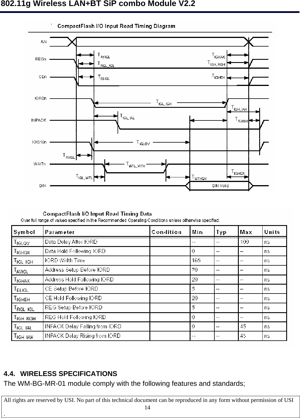
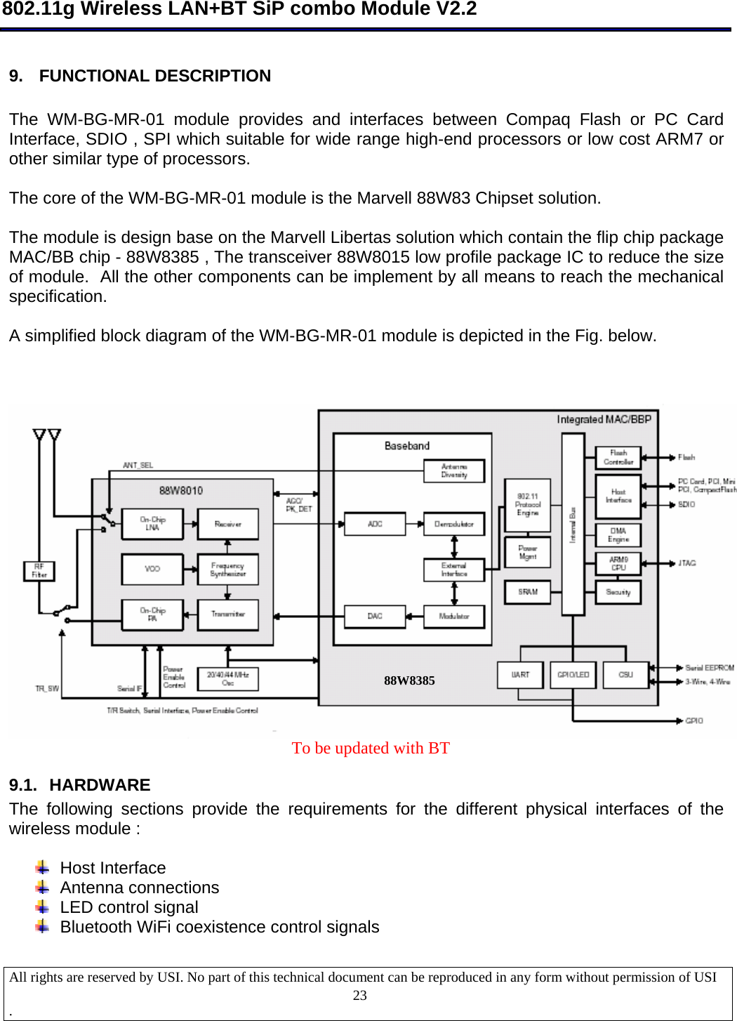
![802.11g Wireless LAN+BT SiP combo Module V2.2 All rights are reserved by USI. No part of this technical document can be reproduced in any form without permission of USI . 228.5. PRODUCT MARKING The Module is marked by laser marking which containing the following information: Description: WM-BG-XX-XX Serial number: yyllwkxxxx Revision: format to follow USI revision level in PDM System For the serial number the following format will be followed: yy = last two digits of current year ll = Assembly Location: UT = USI Taiwan UM = USI Mexico UC = USI China wk = current week (week period = starting on Monday) xxxx = consecutive number, starting at 0000 at beginning of each week. 8.6. ENVIRONMENTALLY SAFE MATERIAL RESTRICTIONS The use of polychlorinated biphenyls (PCB’s) is prohibited (specifically) as dielectric in capacitors or transformers. Electrolytic capacitors shall not be composed of any quaternary salt ammonium and/or gamma-butyrolactone (i.e. no el caps allowed). No CFC's (chlorofluorocarbons) shall be used anywhere in the manufacture of this product. The use of tantalum capacitors should be minimized in any product of the product family [including the power-supply]. Where the use of tantalum caps cannot be avoided, provisions must be made in the manufacturing process to prevent reverse polarization. The WM-BG-MR-01 module hardware design should take the safety of operation into consideration and prevent the potential risk on Labor safety for manufacturing process.](https://usermanual.wiki/General-Dynamics-Itronix/IX100XUSI-WLBT.integrator-manual/User-Guide-712216-Page-22.png)
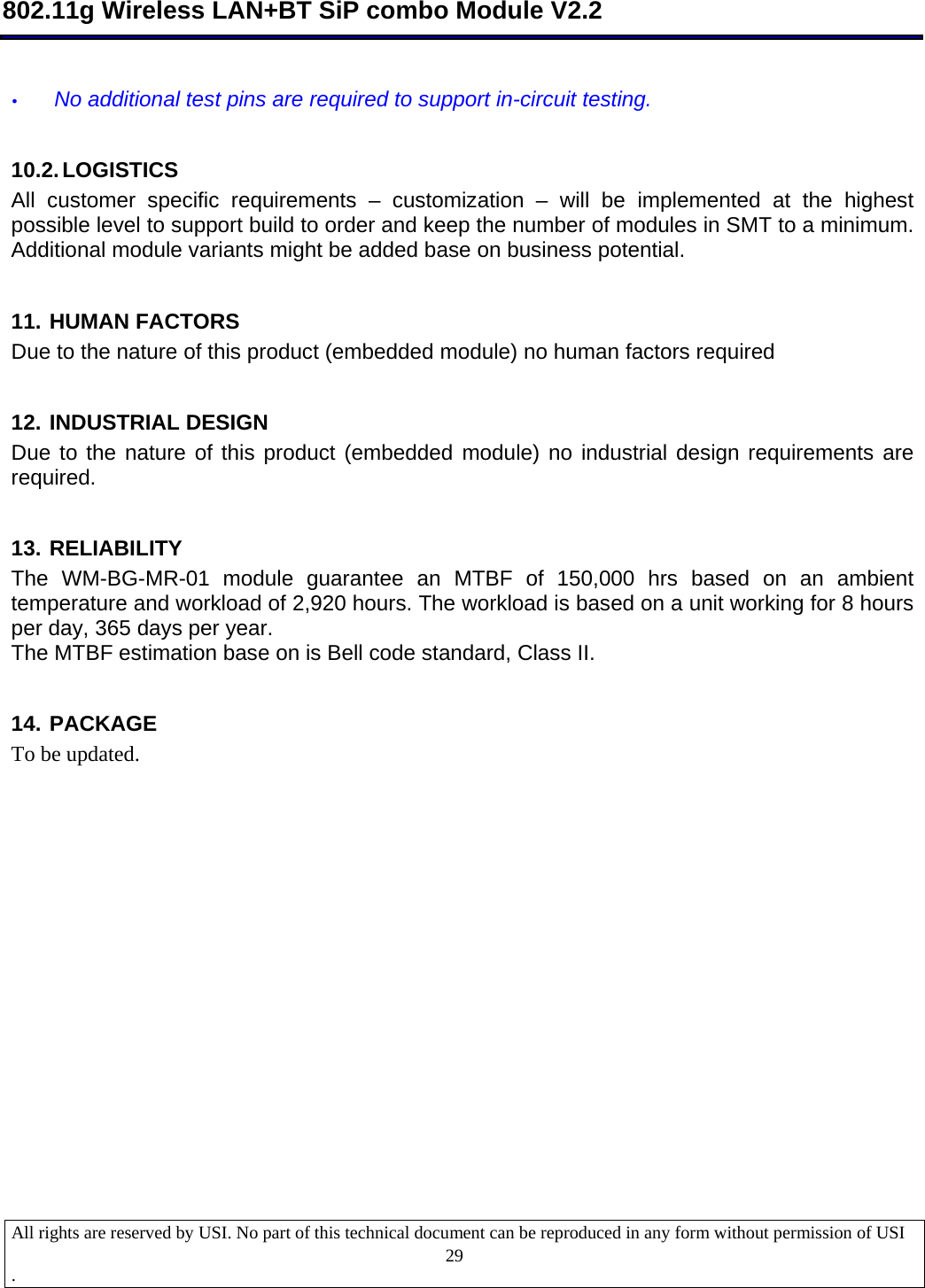
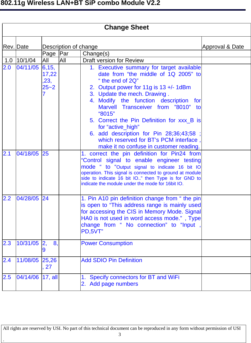
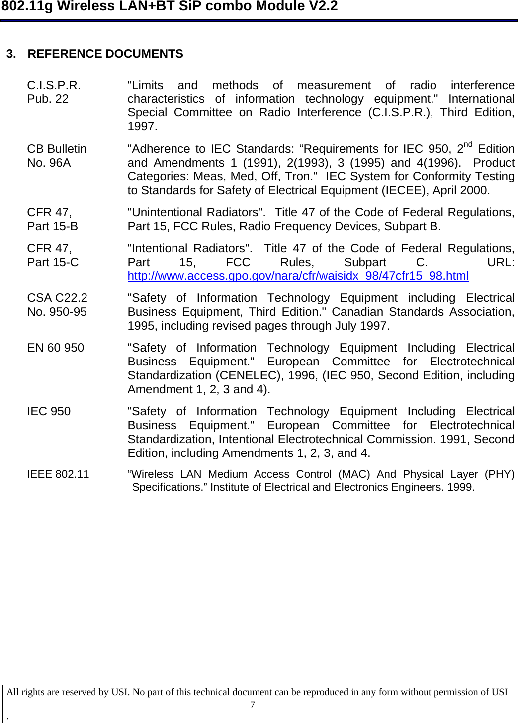
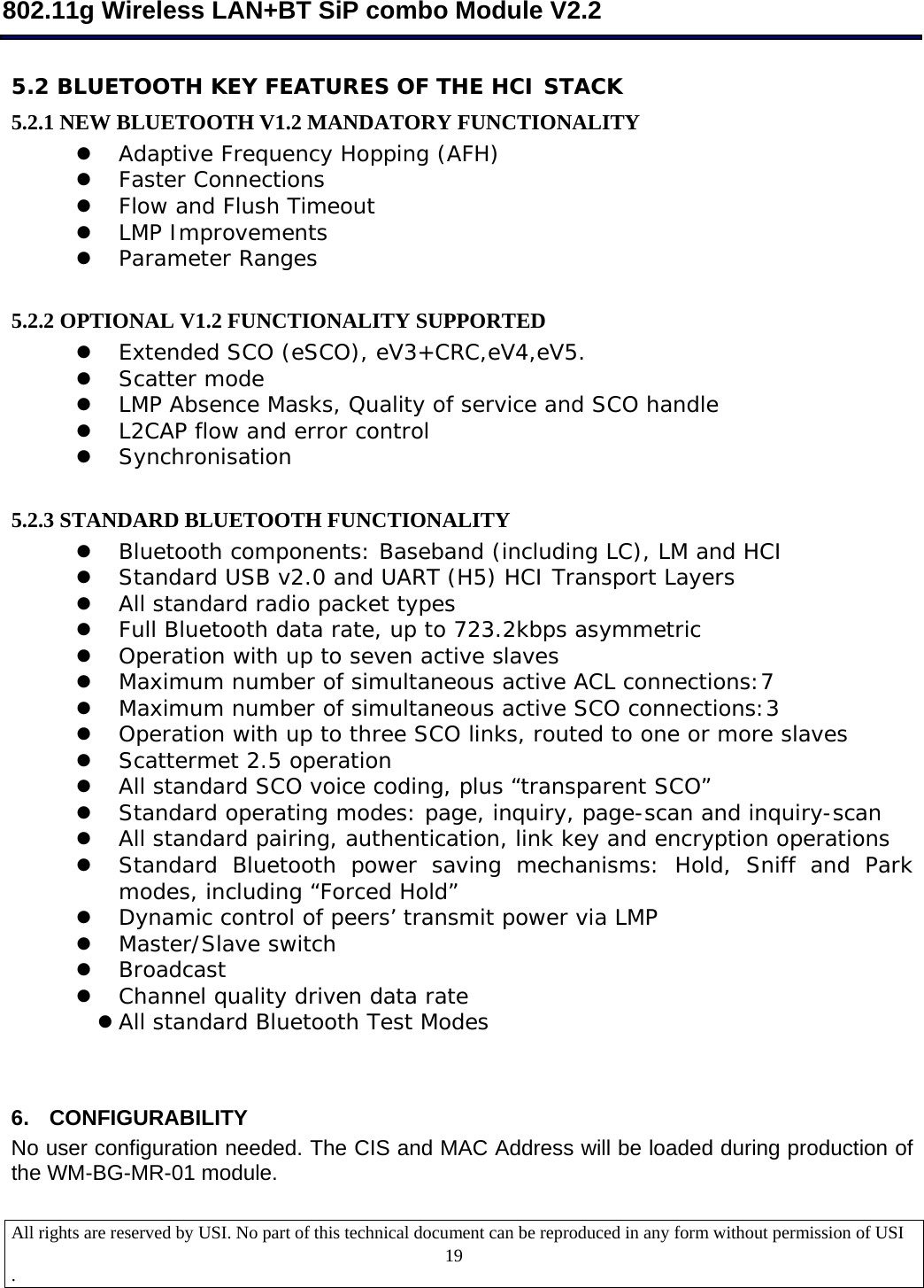
![802.11g Wireless LAN+BT SiP combo Module V2.2 All rights are reserved by USI. No part of this technical document can be reproduced in any form without permission of USI . 24 Power GND 9.2. HOST INTERFACE The host interface will be compatible with CompactFlash (PCMCIA) standard, 16 bit I/O bus. Signals which are not used won’t be routed to the physical interface (connector). The host interface of Combo SiP Bluetooth portion is compliant with UART interface, the default baud rate setting is 115.2kbps and the optional range is from 9.6kbps to 921.6kbps. On Board connector Molex 53794-0608 or 55560-0607 [Socket, 60 pins, with positioning protection, stack height which is able to support 1.5 mm] Datasheet_Molex_53794-0608.pdf Datasheet_Molex_55560-0607.pdf Host System: Host System Connector Molex 54722-0607 [Header, 60 pins, with positioning protection, stack height 1.5mm] Datasheet_Molex_54722-0607.pdf Pin definition [ …] means optional function of the pin. PD : Signal pull down internally in the chip by 50K ohm while initialization. PU : Signal pull up internally in the chip by 100K ohm while initialization. 5VT: 5 Volt tolerance pin xxx_B : Signal pins end with _B are “active high” Pin # Definition Draft Description Type WM-BG-MR-01 CF+ interface 1 GND GND GND 2 D03 HD3 CompactFlash Data bit[3] IO, PU, 4mA 3 D04 HD4 CompactFlash Data bit[4] IO, PU, 4mA 4 D05 HD5 CompactFlash Data bit[5] IO, PU, 4mA](https://usermanual.wiki/General-Dynamics-Itronix/IX100XUSI-WLBT.integrator-manual/User-Guide-712216-Page-24.png)
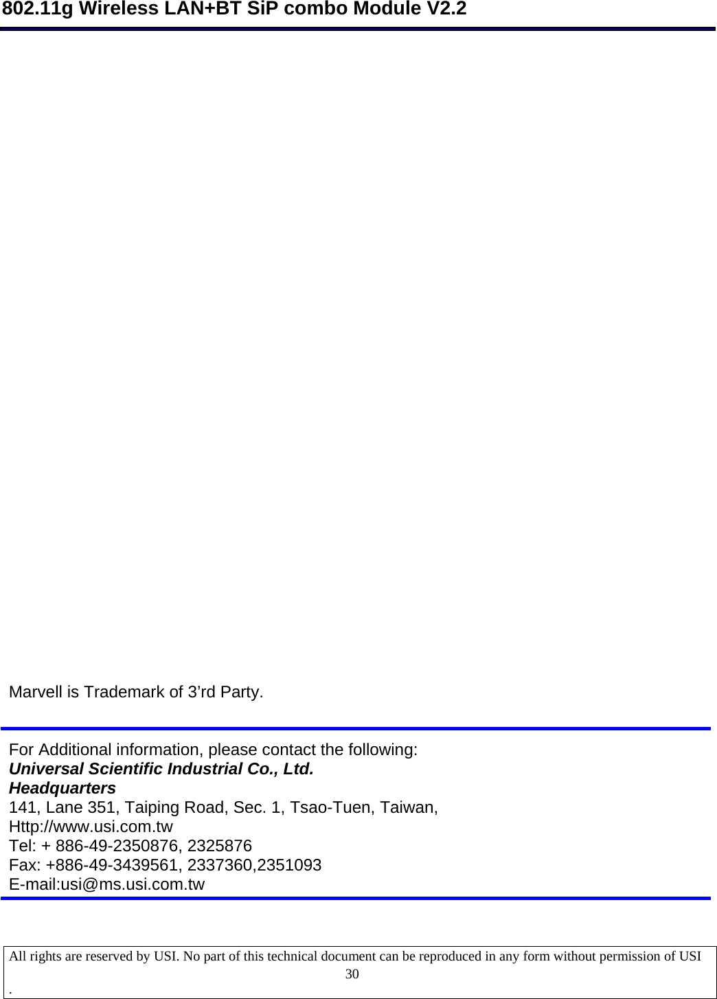
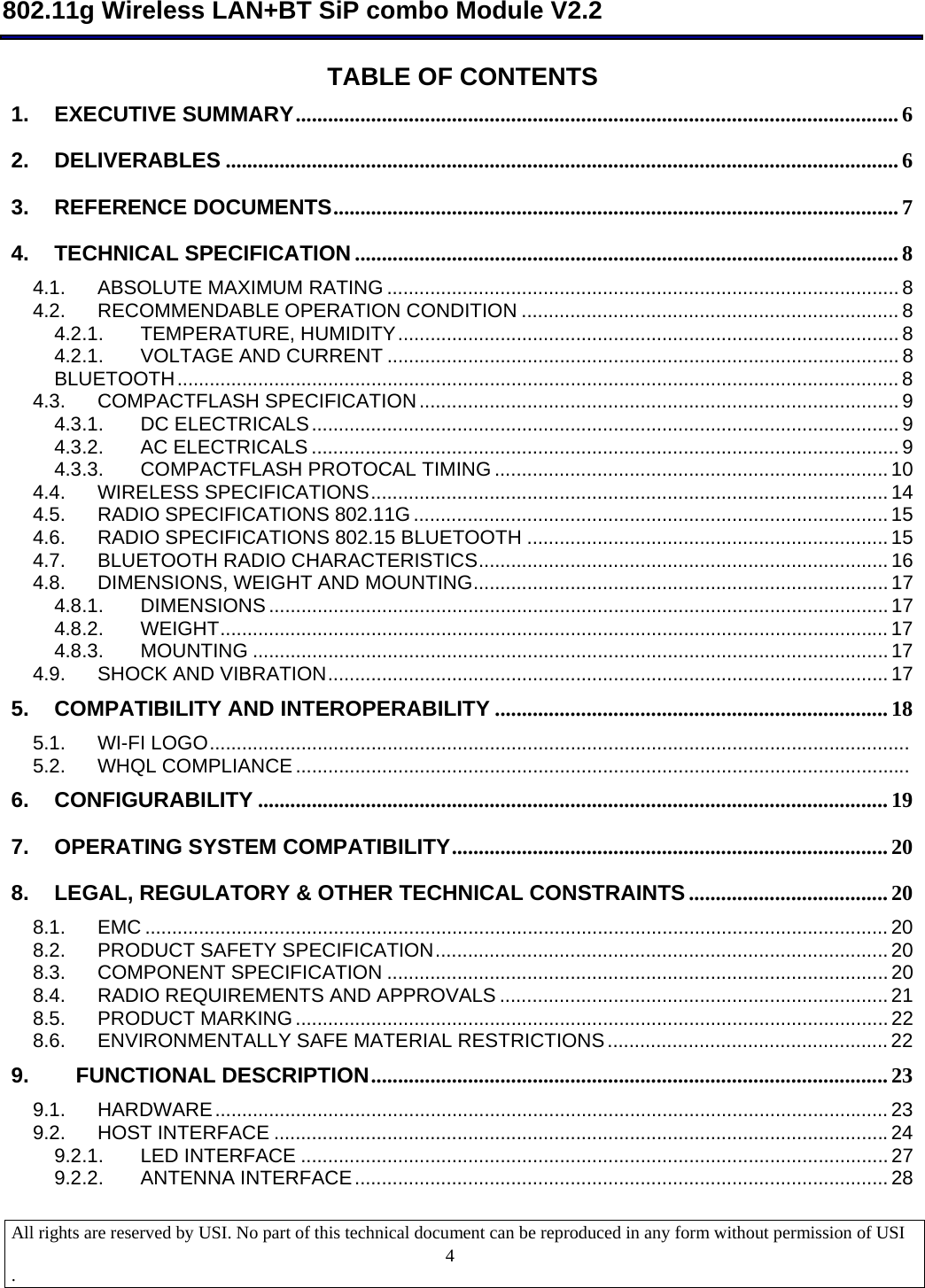
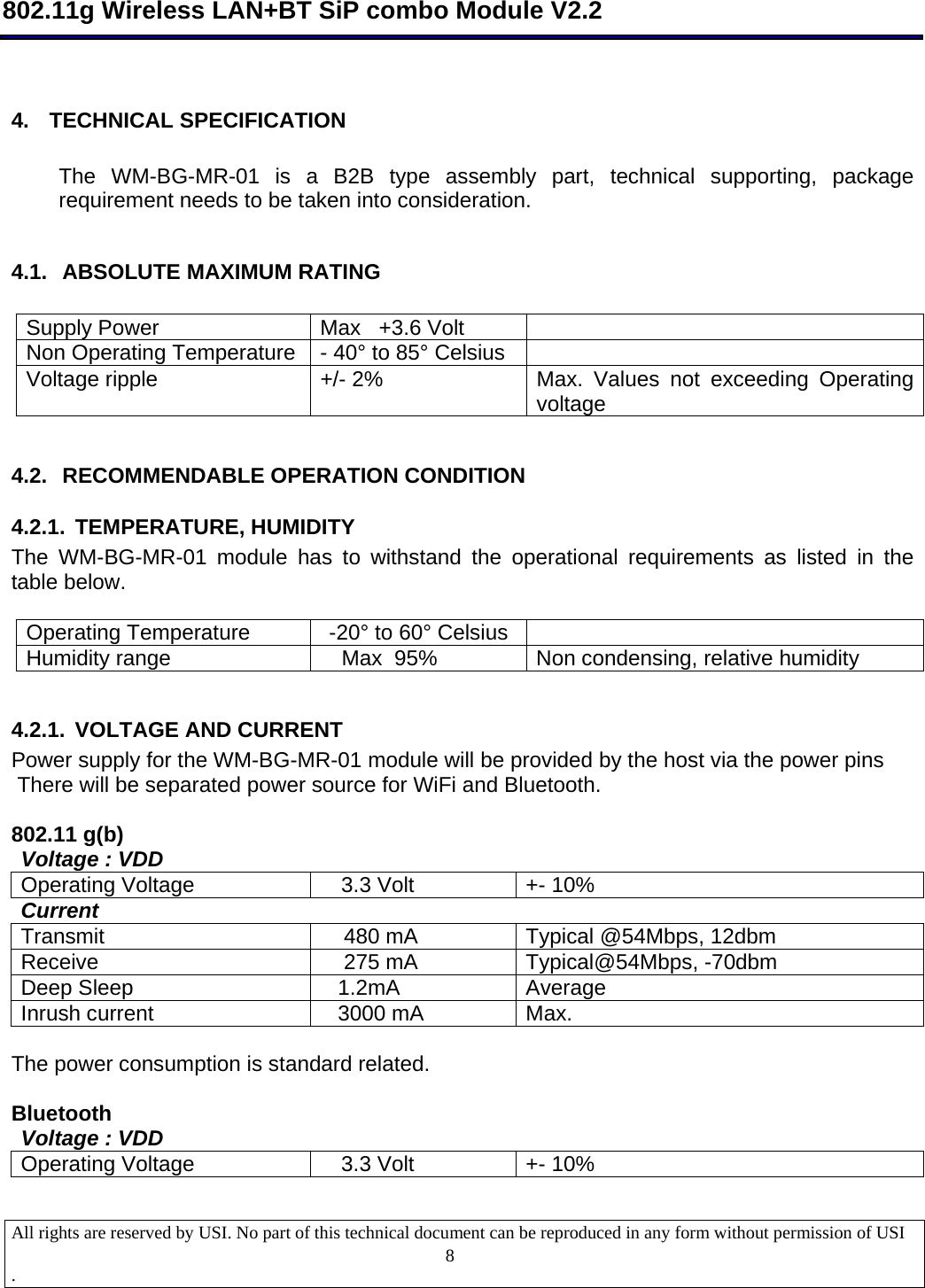
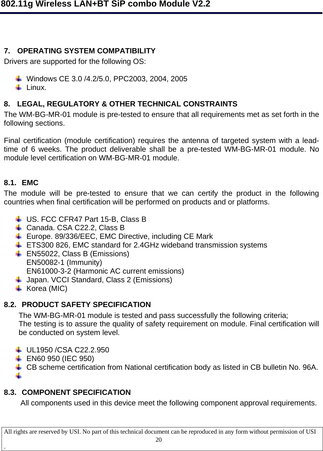
![802.11g Wireless LAN+BT SiP combo Module V2.2 All rights are reserved by USI. No part of this technical document can be reproduced in any form without permission of USI . 255 D06 HD6 CompactFlash Data bit[6] IO, PU, 4mA 6 D07 HD7 CompactFlash Data bit[7] IO, PU, 4mA 7 -CE_1 HCE1_B Card Enable1 is driven by the hostsystem and is used as select strobe inboth I/O and memory mode. Enableseven numbered address bytes. Input, PU 8 A10 HA10 CompactFlash Address bit [10]. Seeaddress bit [0] description. Input, PU 9 -OE SD_CMD HOE_B OUTPUT ENABLE is driven by the hostduring a memory Read Access. SD_CMD : SDIO Command Line Input, PU 10 A09 SD_DAT2 HA9 CompactFlash Address bit [9]. Seeaddress bit [0] description. SD_DATA2 : SDIO DATA LINE 2 Input, PU 11 A08 HA8 CompactFlash Address bit [8]. Seeaddress bit [0] description. Input, PU 12 A07 HA7 CompactFlash Address bit [7]. Seeaddress bit [0] description. Input, PU 13 VCC VCC_WLAN 3.3V supply voltage for WLAN Input 3.3 V 14 A06 HA6 CompactFlash Address bit [6]. Seeaddress bit [0] description. Input, PU 15 A05 HA5 CompactFlash Address bit [5]. Seeaddress bit [0] description. Input, PU 16 A04 HA4 CompactFlash Address bit [4]. Seeaddress bit [0] description. Input, PU 17 A03 HA3 CompactFlash Address bit [3]. Seeaddress bit [0] description. Input, PU 18 A02 HA2 CompactFlash Address bit [2]. Seeaddress bit [0] description. Input, PU 19 A01 HA1 CompactFlash Address bit [1]. Seeaddress bit [0] description. Input, PU 20 A00 HA0 CompactFlash Address bit [0]. Theaddress lines A[10:00] along with the REG signal are used to select thefollowing: • The I/O port address register • The memory mapped port addressregister • A byte in the card's informationstructure (CIS) Input, PU 21 D00 HD0 CompactFlash Data bit[0] IO, PU, 4mA 22 D01 HD1 CompactFlash Data bit[1] IO, PU, 4mA 23 D02 HD2 CompactFlash Data bit[2] IO, PU, 4mA 24 -IOIS16 HIOIS16_B I/O port is 16bits Out, 6mA 25 -CD2 CD2 Normal operation, this pin is functionally for card detection. Out, 6mA 26 N/A TXD_B UART Data output, Active High Output, WPU, 1µA 27 N/A RTS_B UART Request to send, Active low, Tristatable, Pulled-up Output, WPU, 1µA 28 N/A PCM_In Synchronous Data input 29 N/A VCC_WLAN 3.3V power supply for WLAN Input](https://usermanual.wiki/General-Dynamics-Itronix/IX100XUSI-WLBT.integrator-manual/User-Guide-712216-Page-25.png)
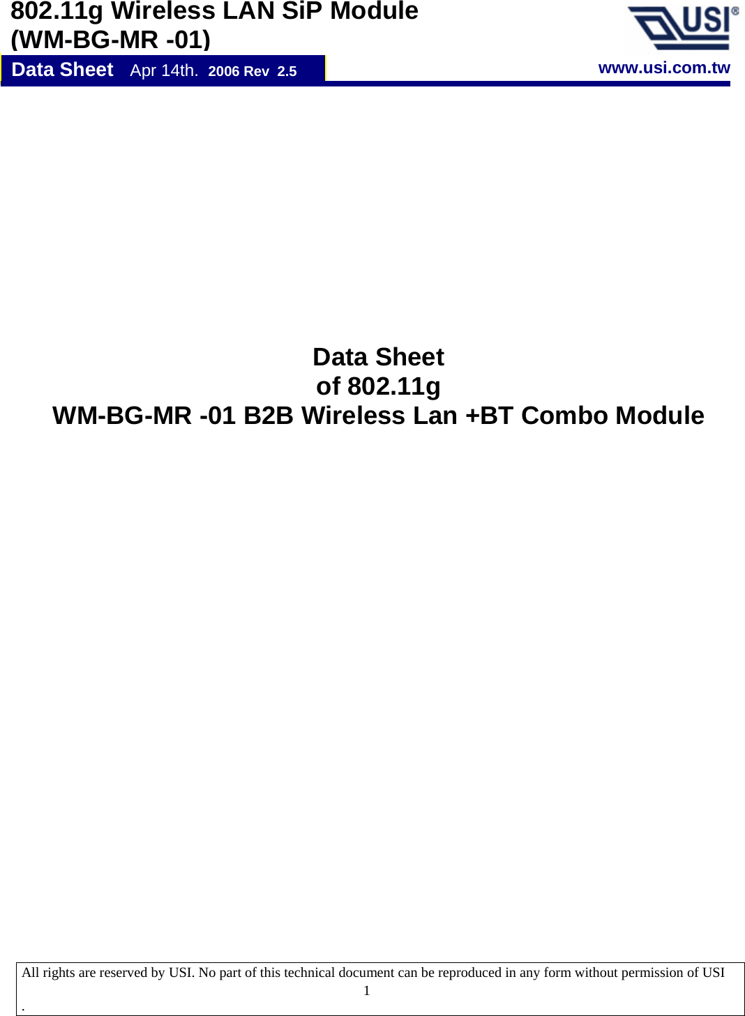
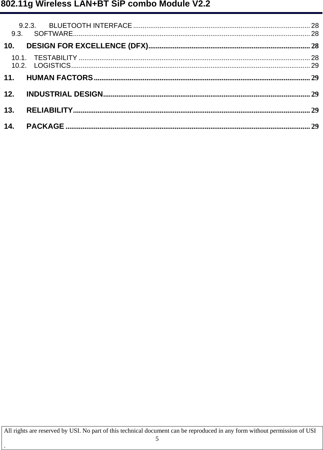
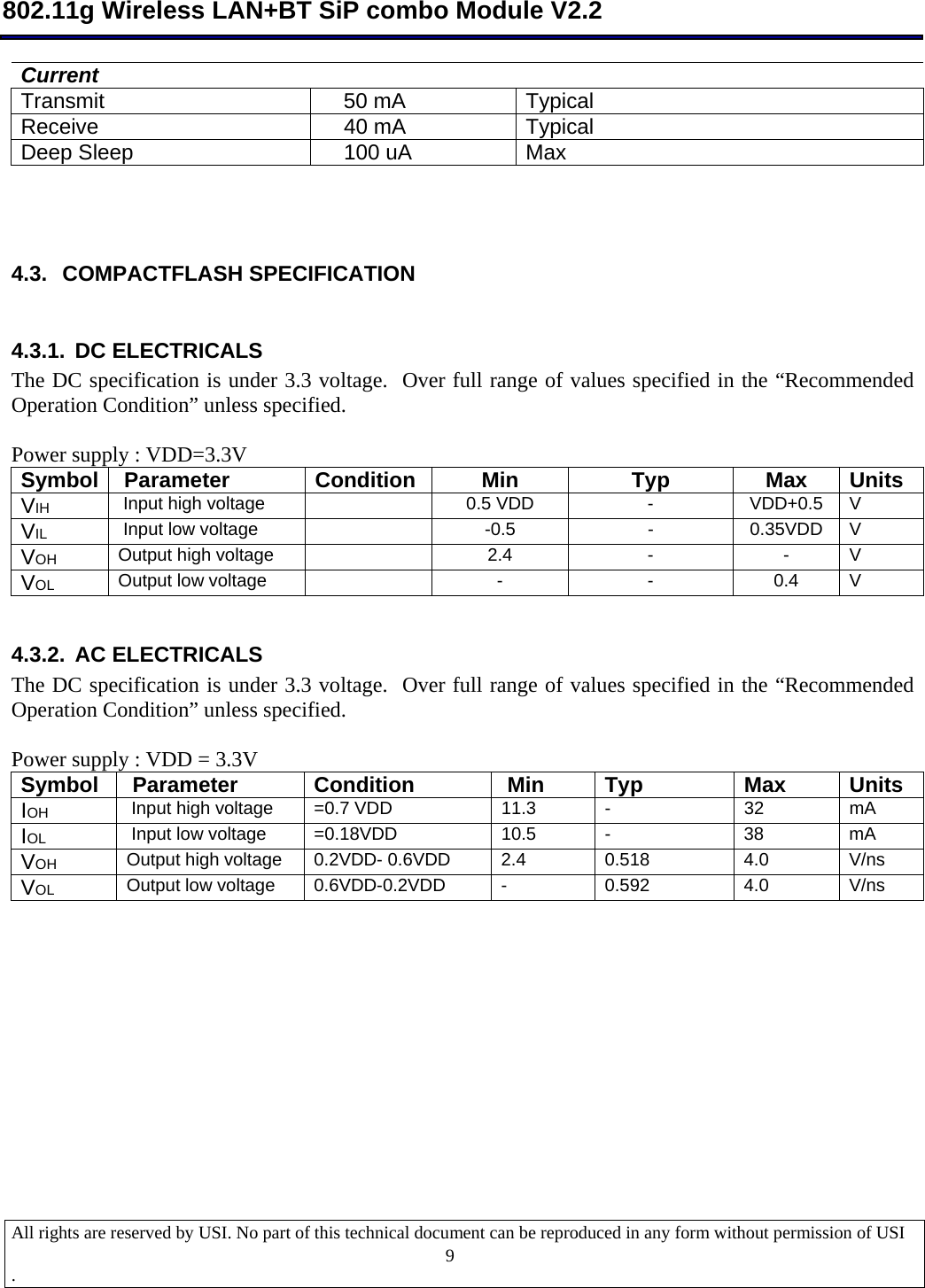
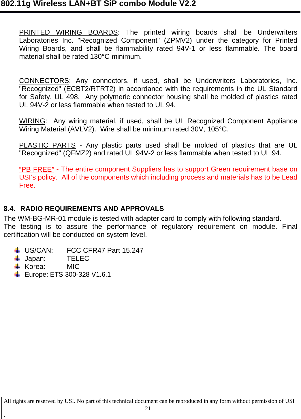
![802.11g Wireless LAN+BT SiP combo Module V2.2 All rights are reserved by USI. No part of this technical document can be reproduced in any form without permission of USI . 2630 GND GND 31 GND GND 32 D10 HD10 CompactFlash Data bit[10] IO, PU, 4mA 33 D09 HD9 CompactFlash Data bit[9] IO, PU, 4mA 34 D08 HD8 CompactFlash Data bit[8] IO, PU, 4mA 35 -STSCHG HSTSCHG_B Card status changed Output, 4mA 36 -SPKR PCM_Sync Synchronous Data strobe Input PD, 4mA 37 -REG HREG_B Register select and I/O enable Input, PU 38 -INPACK HINPACK_B INPUT ACKNOWLEDGE is driven by WM-BG-MR-01. Is asserted when the device is selected and the device is responding to an I/O Read command. Output, 2mA 39 -WAIT HWAIT_B HWAIT_B is driven by WM-BG-MR-01 and allows for extending the memory or I/O cycle Output, 4mA 40 RESET HRESET Used to asynchronously reset WLAN.High active. Input, PU 41 N/A N/A Reserved. Keep connection open on Hostside N/A 42 N/A WLAN_LED_B WLAN LED control signal, driven the LEDindicating the link status of WLAN. Activelow. Output, 4mA 43 N/A PCM_OUT Synchronous Data output 44 IREQ IREQ_B Ready/Busy or Interrupt request. In memory mode, this signal indicatesthe ready or busy status of the card.When held high, the card is ready toaccept a new data transfer. When heldlow the card is busy. In I/O mode, this signal is used to indicate an interrupt condition. Output, 4mA 45 -WE HWE_B WRITE ENABLE is driven by the hostduring a memory Write Access Input, PU 46 -IOWR SD_DAT3 HIOWR_B I/O Write Strobe is driven by the hostand is asserted when the host wants towrite to an on-chip I/O register SD_DAT3 : SDIO DATA LINE 3 Input, PU 47 -IORD SD_DAT1 HIORD_B I/O Read Strobe is driven by the hostand is asserted when the host wants toread from an on-chip I/O register SD_DAT1 : SDIO DATA LINE 1 Input, PU 48 -VS1 -VS1 This pin is connected to Ground onmodule to indicate the voltage of thismodule is 3.3V card. GND 49 -CE2 SD_CLK HCE2_B CARD ENABLE2 is driven by the hostsystem and is used as select strobe inboth I/O and memory mode. Enables oddnumbered address bytes SD_CLK : SDIO CLOCK Input, PU](https://usermanual.wiki/General-Dynamics-Itronix/IX100XUSI-WLBT.integrator-manual/User-Guide-712216-Page-26.png)
![802.11g Wireless LAN+BT SiP combo Module V2.2 All rights are reserved by USI. No part of this technical document can be reproduced in any form without permission of USI . 2750 D15 HD15 CompactFlash Data bit[15] IO, PU, 4mA 51 D14 HD14 CompactFlash Data bit[14] IO, PU, 4mA 52 D13 HD13 CompactFlash Data bit[13] IO, PU, 4mA 53 D12 HD12 CompactFlash Data bit[12] IO, PU, 4mA 54 D11 HD11 CompactFlash Data bit[11] IO, PU, 4mA 55 N/A BT_LED_B BT LED control signal which drives theLED to indicate the activity of Bluetooth.Active low. Output, 4mA 56 N/A RXD_B UART Data input, active High, Pulled down (weak) Input, WPD, 1µA 57 N/A CTS_B UART Clear to Send, Active low, Pulled down (weak) Input, WPD, 1µA 58 N/A SD_DAT0 PCM_CLK Synchronous Data clock SD_DAT0 : SDIO DATA LINE 0 59 N/A VCC_BT 3.3V supply voltage for Bluetooth Input 60 GND GND Fig 1: Pin 1 assignment and indication Drawing ( To be updated with latest design) 9.2.1. LED INTERFACE The Wireless Module will provide two control signals to the host and capable to drive an LED to indicate the connectivity and operating status. The WM-BG-MR-01 have 2 LED’s (output) via 60 pins connector for feedback to the user on the current WLAN activity state. The signaling will reflect status / activity as described in the table below. Those two signals are provided via the board to board connector with the following pin assignment. Pin No Pin description Function description Pin 59Pin 60Pin 59 Pin 1 Pin 60](https://usermanual.wiki/General-Dynamics-Itronix/IX100XUSI-WLBT.integrator-manual/User-Guide-712216-Page-27.png)