H and T Intelligent Control HET-BC1024 Bluetooth Module User Manual
Shenzhen H&T; Intelligent Control Co., Ltd. Bluetooth Module Users Manual
UserManual.wiki
>
H and T Intelligent Control
>
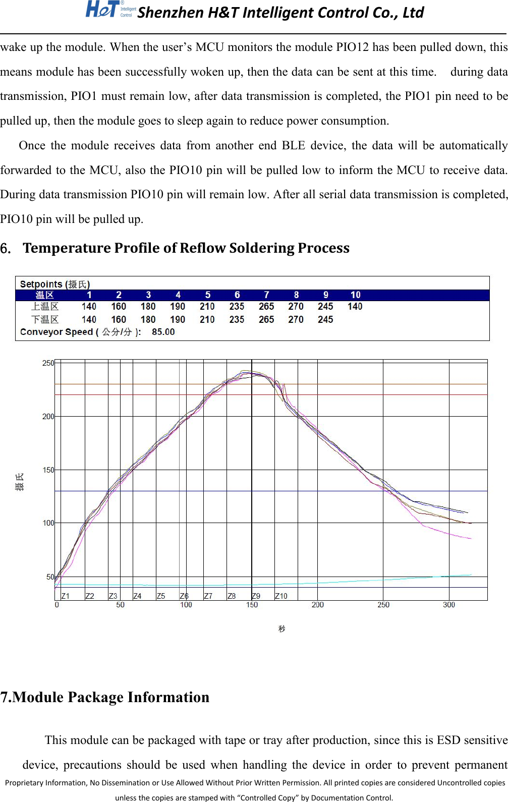
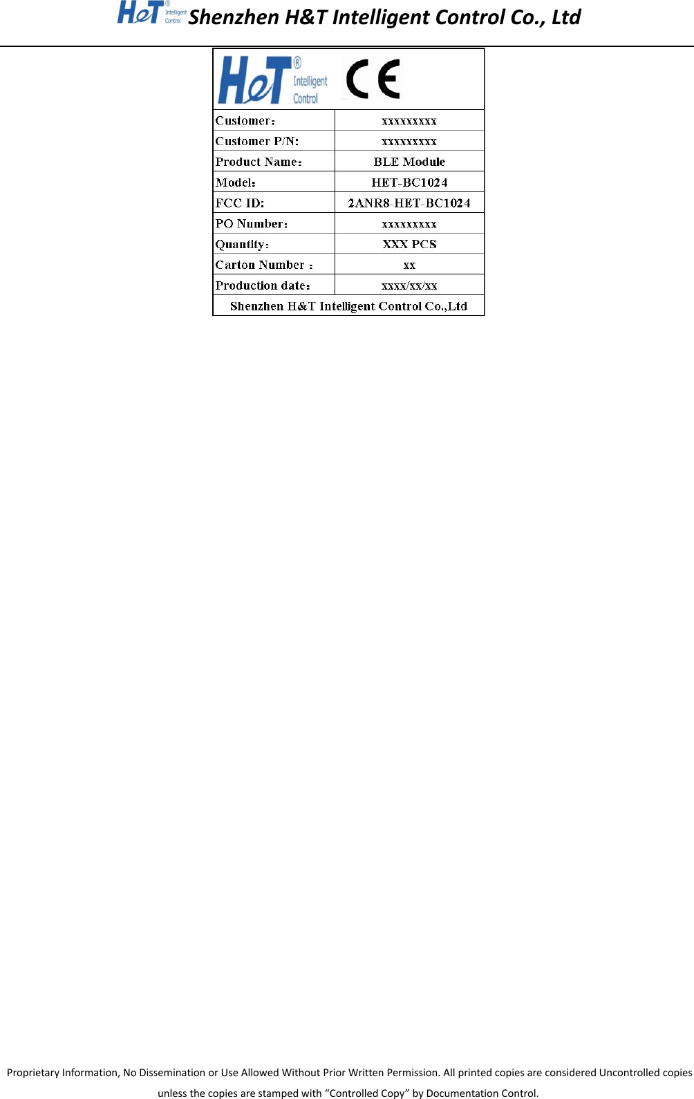
HET BC1024 User Manual
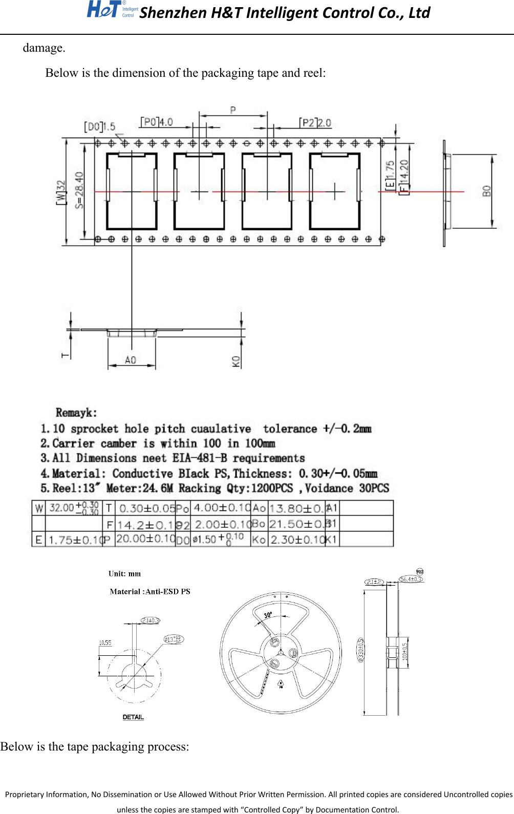
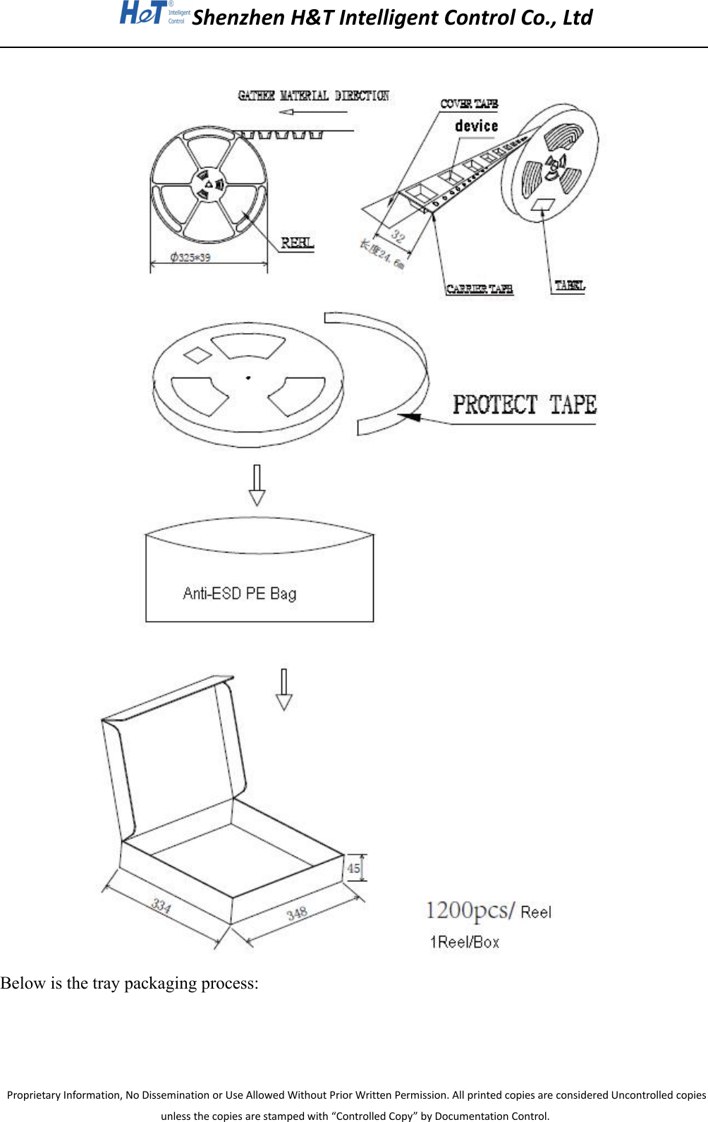
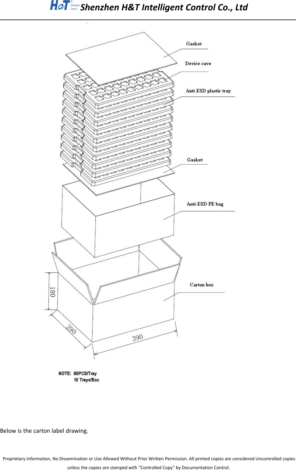
Users Manual
Navigation menu
Upload a User Manual
Namespaces
Wiki Guide
HTML
PDF
Info
Views
User Manual
Discussion / Help
Navigation
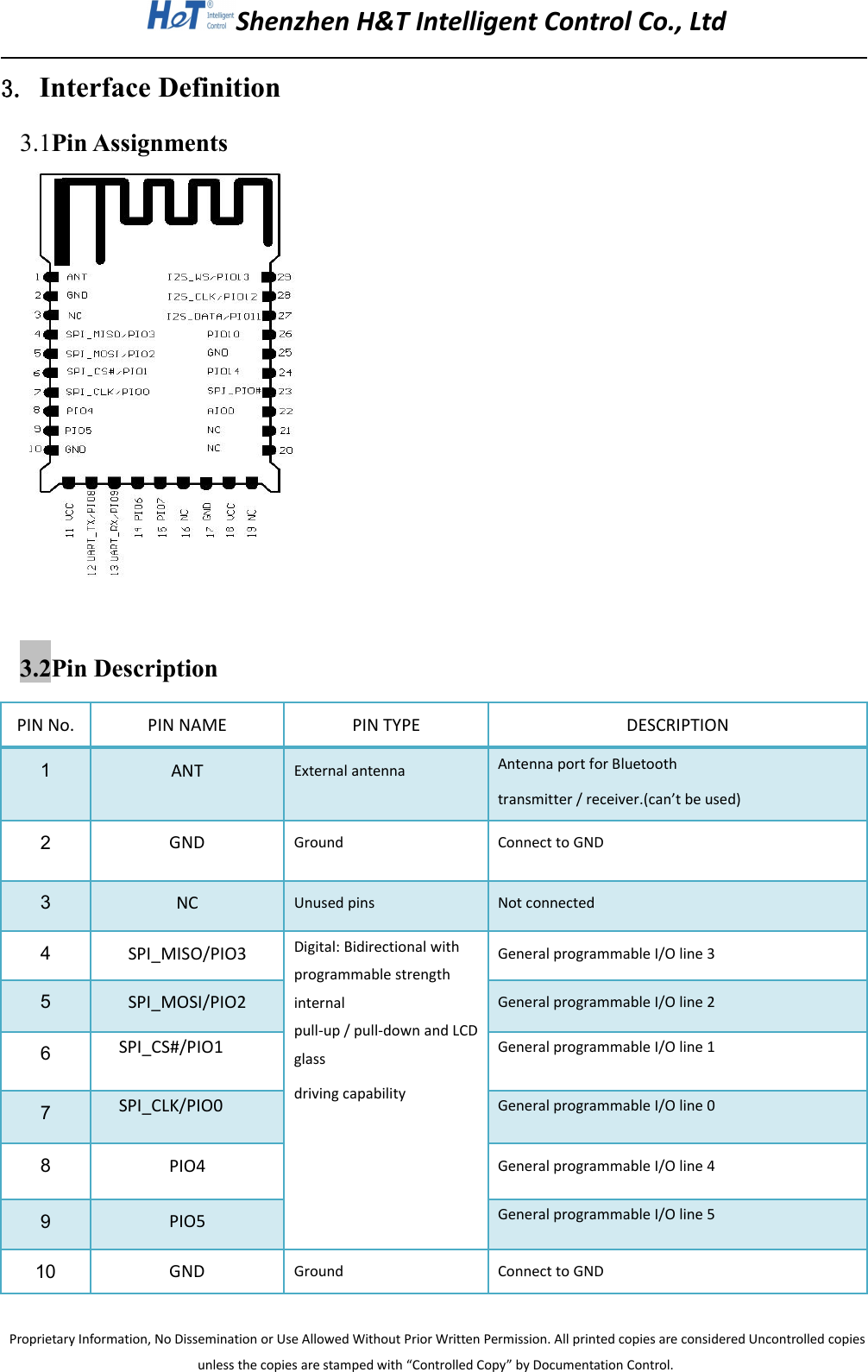
![Shenzhen H&T Intelligent Control Co., LtdProprietary Information, No Dissemination or Use Allowed Without Prior Written Permission. All printed copies are considered Uncontrolled copiesunless the copies are stamped with “Controlled Copy” by Documentation Control.11VCC3V3power-supply connection12UART_ TX/PIO8Digital: Bidirectionalwithprogrammable strengthinternalpull-up / pull-down andLCD glassdriving capabilityGeneral programmable I/O line 813UART_ RX/PIO9General programmable I/O line 914PIO6General programmable I/O line 615PIO7General programmable I/O line 716NCUnused pinsNot connected17GNDGroundConnect to GND18VCC3V3power-supply connection19NCUnused pinsNot connected20NCUnused pinsNot connected21NCUnused pinsNot connected22AIO0Unidirectional analogueAnalogue programmable inputline23SPI_PIO#Input with stronginternal Pull-downSelects Debug SPI on PIO[3:0]24PIO14Digital: Bidirectionalwithprogrammable strengthinternalpull-up / pull-down andLCD glassdriving capabilityGeneral programmable I/O line 1425GNDGroundConnect to GND26PIO10Digital: Bidirectionalwithprogrammable strengthinternalpull-up / pull-down andLCD glassdriving capabilityGeneral programmable I/O line 1027I2S_DATA/PIO11General programmable I/O line 1128I2S_CLK/PIO12General programmable I/O line 1229I2S_WS/PIO13General programmable I/O line 13](https://usermanual.wiki/H-and-T-Intelligent-Control/HET-BC1024/User-Guide-3672666-Page-4.png)