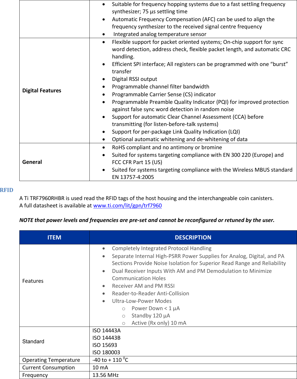
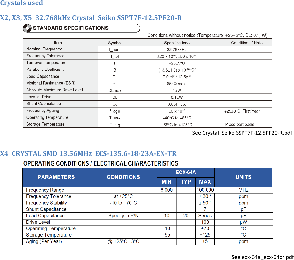
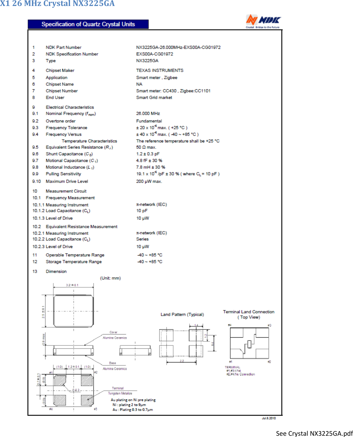
IPS Group IPS2010M800 Multiple Space Parking Meter Controller Module User Manual

IPS Group Inc. Multiple Space Parking Meter Controller Module

User Manual

        Technical Overview IPS Multi Space Parking Meter Controller Module (MSCM)
 RF Exposure Rules and Regulations:    The system antenna(s) used for this transmitter must be installed to provide a separation distance of at least 20 cm from all the persons and must not be co-located or operating in conjunction with any other antenna or transmitter, except in accordance with FCC and Industry Canada multi-transmitter product procedures.    The system antenna(s) used for this module must not exceed 10dBi (CDMA BC0) and 9.31dBi (CDMA BC1) for mobile and fixed operating configurations. Users and installers must be provided with antenna installation instructions and transmitter operating conditions for satisfying RF exposure compliance. The enclosed hardware device complies with Part 15 of the FCC Rules. Operation is subject to the following two conditions: (1) This device may not cause harmful interference, and (2) This device must accept any interference received including interference that may cause undesired operation.   Warning (Part 15.21)  Changes or modifications not expressly approved by IPS Group, Inc. could void the user’s authority to operate the equipment. Manufacturer is not responsible for any radio or TV interference caused by unauthorized modifications to this equipment.   Compliance Statement (Part 15.105(b))  This equipment has been tested and found to comply with the limits for a Class B digital device, pursuant to Part 15 of the FCC Rules. These limits are designed to provide reasonable protection against harmful interference in a residential installation. This equipment generates, uses and can radiate radio frequency energy and, if not installed and used in accordance with the instructions, may cause harmful interference to radio communications. However, there is no guarantee that interference will not occur in a particular installation. If this equipment does cause harmful interference to radio or television reception, which can be determined by turning the equipment off and on, the user is encouraged to try to correct the interference by one or more of the following measures:   • Reorient or relocate the receiving antenna  • Increase the separation between the equipment and receiver  • Connect the equipment into an outlet on a circuit different from that to which the receiver is connected  • Consult the dealer or an experienced radio/TV technician for help   Industry Canada (IC) regulatory information  This device complies with Industry Canada license-exempt RSS standard(s). Operation is subject to the following two conditions: (1) this device may not cause interference, and (2) this device must accept any interference, including interference that may cause undesired operation of the device.   Le présent appareil est conforme aux CNR d'Industrie  Canada applicables aux appareils radio exempts de licence. L'exploitation est autorisée aux deux conditions suivantes : (1) l'appareil ne doit pas produire de brouillage, et (2) l'utilisateur de l'appareil doit accepter tout brouillage radioélectrique subi, même si le brouillage est susceptible d'en compromettre le fonctionnement.   Class B digital device notice  This Class B digital apparatus complies with Canadian  ICES-003, RSS-Gen and RSS-210.  Cet appareil numérique de la classe B est conforme à  la norme NMB-003, CNR-Gen et CNR-210 du Canada.  IPS GROUP INC November 2013   “To meet the host device labelling requirements, any host equipment incorporating the M800 module must include the FCC ID/IC certification number on the host as follows: Contains FCC ID: SGWIPS2010M800 Contains IC: 11583A-IPS2010M800  Contains FCC ID: RI7UE910NA Contains IC: 5131A-5131A-UE910NA”
  IPS MSCM Overview Module Description This controller module is intended to be used across a number of IPS Multi Space Parking Meter platforms. These platforms include IPS designed multi space parking terminals as well as a number of existing designs that can be upgraded and retrofitted with this IPS technology.  Parking terminals equipped with the MSCM may be configured as Pay and Display, Pay by Space, Pay by Plate and other configurations. The MSCM consist of a large LCD display and a controller section enclosed in a protective mechanical housing.  The controller PCBA supports a number of integrated features and interfaces to a number of optional peripheral units.    1 MSCM Rear View
 Top Level Block Diagram
   Integrated Features and Interfaces  Solar energy harvesting controller.  13.8V battery charger for external  12 VRLA battery.  Low voltage supplies for internal use,  5V, 12V and 24V power supplies for external peripherals.  Three  MSP430 Mixed Signal Microcontrollers  4-way key pad  diagnostic keypad  Beeper for audible feedback  GSM / CDMA  Transceiver module for linkup to IPS servers  C1190 Low Power 315/433/868/915 MHz ISM/SRD bands Transceiver for vehicle sensors, Coin Canister, etc.  TRF7960RHBR 13.56-MHZ RFID Reader System  Graphic LCD with controlled backlight  Secondary low Voltage energy storage for backup and support*  Smart Card Interface  IPS Coin Validator Interface  A 6x6 Keypad matrix for various keypad configurations.  Two RS232 interfaces for Printers, Bank Note Acceptors, etc.  14 pin I/O connector for various sensors  Two 10-way Multi Drop Bus connectors for communication between controller and peripherals such as coin handling units, down light and other controllers. Theory of operation Power Management Solar energy is the standard power source for IPS Multi Space Parking Meters.  Electrical energy is derived from high efficiency solar panels. This input energy is converted by the MSCM to levels suitable charging and maintaining an external 12V valve regulated lead acid (VRLA or sealed) battery system which in turn supplies power for internal power backup, internal circuits and external peripherals. Long term power autonomy is achieved by switching systems off when not in use and by storing surplus energy in a high capacity VRLA battery. An average of one hour of sunshine per day is required to maintain this autonomy. This may vary as the requirements for its lighting systems, connectivity and usage change.   The MSCM provides an additional input for a nominal 12VDC input, normally derived from AC mains or other power systems, to support systems where sufficient solar energy is not available or internal heating elements need to be powered during very cold conditions.    Idle Mode A number of configurable idle screens are displayed during idle mode to reassure and inform the potential user of the operational status of the unit, parking tariffs etc. Other systems, as defined by the configuration of the particular system, remain inactive to conserve energy. Events such an a person approaching the unit, pressing a key, inserting a coin or card or bank note will switch the unit to the active mode. The unit may also link up with the IPS managements systems during this mode if triggered by an alarm condition or to exchange data, configurations or software or to log any outstanding transaction details.
 Active Mode Active mode screens guides the user through the balance of the transaction proses related to the event that triggered this mode. The MSCM continuously manages the power and operation of the connected and configured peripherals. Connection to the backend systems via the GSM / CDMA interface may occur during this mode for card payment authorisations or alarm conditions. Active mode reverts to idle mode on completion of the transaction. Diagnostic Mode Access to this mode is via a diagnostic button on the back of the MSCM or the by the insertion of a valid diagnostic card. Navigation through the diagnostic menus is done via the four primary keypad buttons (+, -, cancel and OK) or via the equivalent four buttons on the back of the MSCM. Access to the diagnostic mode should be cancelled explicitly. A no-activity time out will also cancel this mode. Cash Collection Mode  Cash collection is initiated by the insertion of a valid cash-collector’s card and exchanging the coin box and or bank note stacker.  This event is used to reset associated counters, establish a reconciliation point which is communicated to the back-end and to print a cash collection receipt if configured to do so.  The receipt accompanies the coin box /canister and or bank note stacker as an additional security measure if required by the customer.  Primary and I/O Processors Two linked Ti MSP430F5438 mixed signal microcontrollers form the Primary and I/O Processor pair. The Primary Processor (U43) manages the functions normally associated with single space parking meters such as the user interface, coin validator, card reader, server (back-end system) access, wireless vehicle detection, wireless coin container communications, Host ID (RFID) detection and motion sensing.  The I/O Processor (U20) manages the additional functions associated with multi space parking meters such as the receipt printer, bank note acceptor different keypad configurations, coin handling units, expiry indicators, down light controllers and various cabinet sensors. Full technical information falls outside the scope of this document and can be downloaded from www.ti.com/product/msp430f5438 3-AXIS DIGITAL COMPASS A Honeywell HMC5983 (U57) is a temperature compensated three-axis integrated circuit magnetometer and is used to sense the MSCM’s orientation and motion. http://www51.honeywell.com/aero/common/documents/myaerospacecatalog-documents/Defense_Brochures-documents/HMC5983_3_Axis_Compass_IC.pdf  3-AXIS ACCELEROMETER The Xtrinsic MMA8453Q 3-Axis, 10-bit/8-bit Digital Accelerometer (U23) supplements and enhances the functions performed by the 3-axis digital compass (U57) www.freescale.com/files/sensors/doc/data_sheet/MMA8453Q.pdf   I/O Sensors (H4) This 14-way bus provides I2C comms, Connection for an external 25VP-P Piezo buzzer, and eight discrete switches to GND. The switches are used to sense the status of various doors and locks in the cabinet. To conserve power these lines
 are not permanently powered (i.e. not pulled up) but rather pulsed periodically to sense its status. A ‘high’ will be read back from an internal sense capacitor if the switch is open and a ‘ low’ if switched to GND. MODBUS1&2 (MB1 & MB2) These two linked headers provides controlled V_BAT (+3.6V) and V_MAIN_BAT (+12V) and a communication channel to a number of peripherals in a multidrug topology. Peripherals on this bus include a human proximity detector, expiry indicator, coin handling unit etc. KEYPADS (H7) H7 is a 20-way header providing V_BAT (+3.6V),  V_KBD_BK_LED  (switched +3.6V) for keypad backlighting and an 8-Col x 8-Row keypad matrix. This allows any number of keypads to be daisy chained and each keypad to be individually mapped to a 64 position key map. Printer Power (H10) and Printer Data Port  The printer power header (H10) provides high capacity switched +5V, +12V and +24V suitable for supplying single or double sided thermal paper receipt printers. The printer data port header provides a bidirectional RS232 communication link between the receipt printer and the MSCM. Bank Note Acceptor Power (H9) and Note Data Port  The BNA power header (H9) provides high capacity switched +5V, +12V and +24V suitable for supplying Bank Note Acceptors (BNA’s). The NOTE DATA port header provides a bidirectional RS232 communication link as well as a logic level pulsed communication channel between the BNA and the MSCM.
 Technical Specifications. NOTE that power levels and frequencies are pre-set and cannot be reconfigured or retuned by the user. Main Battery Connection PARAMETERS CONDITIONS MIN TYP MAX UNITS Charge Voltage to Battery Sufficient Solar or EXT Power  13.8  Volt Charge Current to Battery “   500 mA Current Demand from Battery Insufficient Solar or EXT Power  5  mA Solar Input PARAMETERS CONDITIONS MIN TYP MAX UNITS Input Voltage Required  6 12 38 Volt Current Demand from Panel Normal Operation Average  5  mA Backup Power Depleted   1000 EXT Power Input PARAMETERS CONDITIONS MIN TYP MAX UNITS Input Voltage Required  6 12 38 Volt Current Demand from Source Normal Operation Average  5  mA Backup Power Depleted   1000 Auxiliary 5V Supply PARAMETERS CONDITIONS MIN TYP MAX UNITS Output Voltage  4.5 5.0 5.5 Volt Available Output Current Continuous  500  mA Peak for 100 ms   5000 Auxiliary 12V Supply PARAMETERS CONDITIONS MIN TYP MAX UNITS Output Voltage  11 12 13 Volt Available Output Current Continuous  500  mA Peak for 100 ms   4000 Auxiliary 24V Supply PARAMETERS CONDITIONS MIN TYP MAX UNITS Output Voltage  22 24 26 Volt Available Output Current Continuous  500  mA Peak for 100 ms   3000
 Graphic Display – General Specifications ITEM DESCRIPTION UNIT LCD type FSTN Positive Transflective - Viewing Angle 6 O’clock Module size (W×H×T) 136.6 × 176.0 × 5.0  mm Viewing area (W×H) 120 × 82.65  mm Viewing angle 6 O’clock  Number of dots 320 × 240  dots Dot size (W×H) 0.31 × 0.31  mm Dot pitch (W×H)  0.325 × 0.325 mm Backlight LED, White  Operating temperature  -4   to   185 -20  to     70 0F 0C Backlight ITEM DESCRIPTION UNIT Technology LED  Colour White  Power Dissipation (MAX) 0.51 W Forward Voltage (Typical) 3.1 V Smart Card Interface This 16-way proprietary interface connects the IPS Card Reader PCBA to the MSCM. Processed magnetic strip data as well as direct access to smartcard chip contacts is achieved through this contact.  Coin Validator Interface This 10-way proprietary interface connects the IPS Coin Validator to the MSCM. This allows for analog and digital signals relating to the coin characteristics being analysed to be communicated to the MSCM for further processing. GSM / CDMA  The primary component for this interface is the Telit UE910-NAD installed in U102.  The UE910 is an HSPA 7.2 Mbps technology member of the xE910 family.   For further information visit http://www.telit.com/en/products/umts.php  UE910-NAD ITEM DESCRIPTION All UE910 variants are dual-band GSM/GPRS/EDGE and dual band UMTS/HSPA Features  Advanced E-GPRS/WCDMA/HSDPA/HSUPA Software protocol stack (Layer 1 to 3) – Version: 3GPP Release 7   GSM Quad band (900/1800 MHz for EUx, 850/1900 MHz for NAx)   WCDMA dual-band: B1&B8 for the EUx models and B2&B5 for the NAx models   HSDPA up 7.2Mbps   HSUPA up to 5.76Mbps   WCDMA up to 384kbps downlink/uplink   DTM (Dual Transfer Mode)   CPC (DRX/DTX) (Continuous Packet Connectivity)   DARP
  Control via AT commands according to 3GPP TS27.005, 27.007 and Telit customized AT commands   Serial port multiplexer 3GPP TS27.010   SIM application Tool Kits 3GPP TS 51.014   Power consumption (typical values)  - Stand-by current 2G, DRX5, 1.1 mA  - Stand-by current 3G, DRX7, 1.2 mA   Output power  - Class 4 (2W) @ 850 / 900 MHz, GSM  - Class 1 (1W) @ 1800 / 1900 MHz, GSM  - Class E2 (0.5W) @ 850/900 MHz, EDGE  - Class E2 (0.4W) @ 1800/1900 MHz, EDGE  - Class 3 (0.25W) @ 850/900/1900/2100 MHz, WCDMA   Sensitivity:  - 109 dBm (typ.) @ 850 / 900 MHz (GSM)  - 110 dBm (typ.) @ 1800 / 1900 MHz (GSM)  - 111 dBm (typ.) @ 850/900/1900 / 2100 MHz (WCDMA)  Data Transmission  HSPA: category 8 in downlink e category 6 in uplink  - DL up to 7.2Mbps  - UL up to 5.76Mbps   WCDMA: up to 384kbps downlink/uplink   Asynchronous non-transparent CSD up to 9.6kbps   GPRS class 10 for NAx variants and class 33 for EUX variants   EDGE class 10 for NAx variants and class 33 for EUX variants   Coding scheme 1 to 4 (GPRS) & Modulation Coding scheme 1 to 9 (EDGE)  Approvals         Temperature Range     -400F  ~ +1850F    (-400C  ~ +850C) RoHS compliance RoHS (Restriction of Hazardous Substances) directive of the European Union (EU directive 2011/65/EU) Operating Frequency The operating frequencies in GSM850, EGSM900, DCS1800, PCS1900, WCDMA modes are compliant to the 3GPP and WCDMA specifications. Mode Freq. TX  (MHz) Freq. RX (MHz) Channels TX - RX offset GSM850 824.2 ~ 848.8 869.2 ~ 893.8 128 ~ 251 45 MHz EGSM900 890.0 ~ 914.8 935.0 ~ 959.8 0 ~ 124 45 MHz 880.2 ~ 889.8  925.2 ~ 934.8  975 ~ 1023  45 MHz  DCS1800 1710.2 ~ 1784.8 1805.2 ~ 1879.8 512 ~ 885 95MHz PCS1900 1850.2 ~ 1909.8 1930.2 ~ 1989.8 512 ~ 810 80MHz WCDMA850 (band V) 826.4 ~ 846.6 871.4 ~ 891.6 Tx: 4132 ~ 4233 Rx: 4357 ~ 4458 45MHz WCDMA900 (band VIII) 882.4 ~ 912.6 927.4 ~ 957.6 Tx: 2712 ~ 2863 Rx: 2937 ~ 3088 45MHz WCDMA1900 (band II) 1852.4 ~ 1907.6 1932.4 ~ 1987.6 Tx: 9262 ~ 9538 Rx: 9662 ~ 9938 80MHz WCDMA2100 (Band I) 1922.4 ~ 1977.6 2112.4 ~ 2167.6 Tx: 9612 ~ 9888 Rx: 10562 ~ 10838 190MHz Transmitter output power The UE910 family transceiver output of GSM/GPRS mode in 850/900MHz bands are class 4 in accordance with the specifications which determine the nominal 2W peak RF power (+33dBm) on 50ohm. In the 1800/1900MHz bands are class 1 in accordance with the specification which determines the nominal 1W peak RF
 power (+30dBm) on 50ohm. The UE910 family transceiver output of EDGE mode in 850/900MHz bands are class E2 in accordance with the specifications which determine the nominal 0.5W peak RF power (+27dBm) on 50ohm. In the 1800/1900MHz bands are class E2 in accordance with the specification which determine the nominal 0.4W peak RF power (+26dBm) on 50ohm.  The UE910 family transceiver output of WCDMA mode in 850/900/1900/2100MHz bands is class 3 in accordance with the specifications which determine the nominal 0.25W peak RF power (+24dBm) on 50ohm. Sensitivity Band Typical Note GSM 850 -109.5 dBm BER Class II  < 2.44 % GSM 900 -109 dBm BER Class II  < 2.44 % DCS 1800 -110 dBm BER Class II  < 2.44 % PCS 1900 -109.5 dBm BER Class II  < 2.44 % WCDMA FDD B1 -111 dBm BER < 0.1 % WCDMA FDD B2 -110 dBm BER < 0.1 % WCDMA FDD B5 -111 dBm BER < 0.1 % WCDMA FDD B8 -110 dBm BER < 0.1 % Antenna   For further information, please refer to the UE910 family Hardware User Guide ANTENNA REQUIREMENTS Frequency range  Depending by frequency band(s) provided by the network operator, the customer shall use the most suitable antenna for that/those band(s)  Bandwidth (GSM/EDGE)  70 MHz in GSM850, 80 MHz in GSM900, 170 MHz in DCS & 140 MHz PCS band  Bandwidth  (WCDMA)  70 MHz in WCDMA Band V  80 MHz in WCDMA Band VIII  140 MHz in WCDMA Band II  250 MHz in WCDMA Band I  Gain  1.4dBi @900 and 3dBi @1800  1.4dBi @850 and 3dBi @1900  1.43 dBi (WCDMA)  Impedance  50 ohm  Input power  > 33dBm(2 W) peak power in GSM  > 24dBm Average power in WCDMA  VSWR absolute max  ≤ 5:1 (limit to avoid permanent damage)  VSWR recommended  ≤ 2:1 (limit to fulfil all regulatory requirements)  Supply voltage Nominal Supply Voltage  3.8V  Operating Voltage Range  3.4 ~ 4.2V  Extended Operating Voltage Range  3.1 ~ 4.5V  Power consumption  Depending on network configuration and not under module control  UE910 Mode Average (mA) Mode Description SWITCHED OFF Module supplied but switched off Switched Off 180uA IDLE mode (WCDMA) AT+CFUN=1 12.2 Normal Mode: full functionality of the module AT+CFUN=5 1.8 Full functionality with power saving; DRX7; Module registered on network can receive incoming calls and SMS IDLE mode (GSM/EDGE) AT+CFUN=1 19 Normal Mode: full functionality of the module
 AT+CFUN=4 16.5 Module is not registered on network AT+CFUN=5 1.2 Full functionality with power saving; DRX9 (1.3mA in case of DRX5) Operative mode (WCDMA) WCDMA Voice 152 WCDMA voice call (TX = 10dBm) WCDMA HSDPA (0dBm) 187 WCDMA data call (Cat 8, TX = 0dBm) WCDMA HSDPA (0dBm) 494 WCDMA data call (Cat 8, TX = 22dBm) Operative mode (EDGE) EDGE 4TX+1RX EDGE Sending data mode GSM 850/900 – G8 495 DCS 1800/ PCS1900 – G7 484 Operative mode (GSM) CSD TX and RX mode GSM VOICE CALL GSM850/900 CSD PL5 220 DCS1800/ PCS 1900 CSD PL0 167 GPRS 4TX+1RX GPRS Sending data mode GSM 850/900 PL5 580 DCS1800/PCS1900 PL0 438 Data Transmission capabilities The UE910 family supports:   HSPA: D/L up to 7.2Mbps, U/L up to 5.76Mbps   Asynchronous non-transparent CSD up to 9.6kbps for GSM, 14.4kbps for WCDMA   EDGE Class 10 for NAx variants and Class 33 for EUx variants   Coding scheme 1 to 4 (GPRS) & Modulation Coding scheme 1 to 9 (EDGE)  Local security management The local security management can be done with the lock of Universal Subscriber Identity Module (USIM), and the security code will be requested at power-up.    Local Radio Based on the Ti CC1101 this sub-1 GHz transceiver designed for very low-power wireless applications. The circuit is mainly intended for the ISM (Industrial, Scientific and Medical) and SRD (Short Range Device) frequency bands at 315, 433, 868, and 915 MHz, but can also be programmed for operation at other frequencies in the 300-348 MHz, 387-464 MHz and 779-928 MHz bands. This wireless system is used for data communications with nearby local systems such as the wireless coin canister electronics. NOTE that power levels and frequencies are pre-set and cannot be reconfigured or retuned by the user. ITEM DESCRIPTION RF Performance  High sensitivity  -116 dBm at 0.6 kBaud, 433 MHz, 1% packet error rate  -112 dBm at 1.2 kBaud, 868 MHz, 1% packet error rate  Low current consumption (14.7 mA in RX, 1.2 kBaud, 868 MHz)  Programmable output power up to +12 dBm for all supported frequencies  Excellent receiver selectivity and blocking performance  Programmable data rate from 0.6 to 600 kbps  Frequency bands: 300-348 MHz, 387-464 MHz and 779-928 MHz Analog Features  2-FSK, 4-FSK, GFSK, and MSK supported as well as OOK and flexible ASK shaping
  Suitable for frequency hopping systems due to a fast settling frequency synthesizer; 75 μs settling time  Automatic Frequency Compensation (AFC) can be used to align the frequency synthesizer to the received signal centre frequency   Integrated analog temperature sensor Digital Features  Flexible support for packet oriented systems; On-chip support for sync word detection, address check, flexible packet length, and automatic CRC handling.  Efficient SPI interface; All registers can be programmed with one “burst” transfer  Digital RSSI output  Programmable channel filter bandwidth  Programmable Carrier Sense (CS) indicator  Programmable Preamble Quality Indicator (PQI) for improved protection against false sync word detection in random noise  Support for automatic Clear Channel Assessment (CCA) before transmitting (for listen-before-talk systems)  Support for per-package Link Quality Indication (LQI)  Optional automatic whitening and de-whitening of data General  RoHS compliant and no antimony or bromine  Suited for systems targeting compliance with EN 300 220 (Europe) and FCC CFR Part 15 (US)  Suited for systems targeting compliance with the Wireless MBUS standard EN 13757-4:2005 RFID A Ti TRF7960RHBR is used read the RFID tags of the host housing and the interchangeable coin canisters. A full datasheet is available at www.ti.com/lit/gpn/trf7960  NOTE that power levels and frequencies are pre-set and cannot be reconfigured or retuned by the user. ITEM DESCRIPTION Features   Completely Integrated Protocol Handling  Separate Internal High-PSRR Power Supplies for Analog, Digital, and PA Sections Provide Noise Isolation for Superior Read Range and Reliability  Dual Receiver Inputs With AM and PM Demodulation to Minimize Communication Holes  Receiver AM and PM RSSI  Reader-to-Reader Anti-Collision  Ultra-Low-Power Modes o Power Down < 1 µA o Standby 120 µA o Active (Rx only) 10 mA Standard ISO 14443A ISO 14443B ISO 15693 ISO 180003  Operating Temperature -40 to + 110 0C Current Consumption 10 mA Frequency 13.56 MHz
 Crystals used X2, X3, X5  32.768kHz Crystal  Seiko SSPT7F-12.5PF20-R     See Crystal  Seiko SSPT7F-12.5PF20-R.pdf.  X4  CRYSTAL SMD 13.56MHz  ECS-135.6-18-23A-EN-TR  See ecx-64a_ecx-64cr.pdf
 X1 26 MHz Crystal NX3225GA  See Crystal NX3225GA.pdf

Navigation menu