Intelligent Distributed Controls ZB100 ZB100 ZigBee Module User Manual ZigBee Ready OEM Modules
Intelligent Distributed Controls Limited ZB100 ZigBee Module ZigBee Ready OEM Modules
UserManual.wiki
>
Intelligent Distributed Controls
>
ZB100 User Manual
>
Manual
Contents
1.
Manual
2.
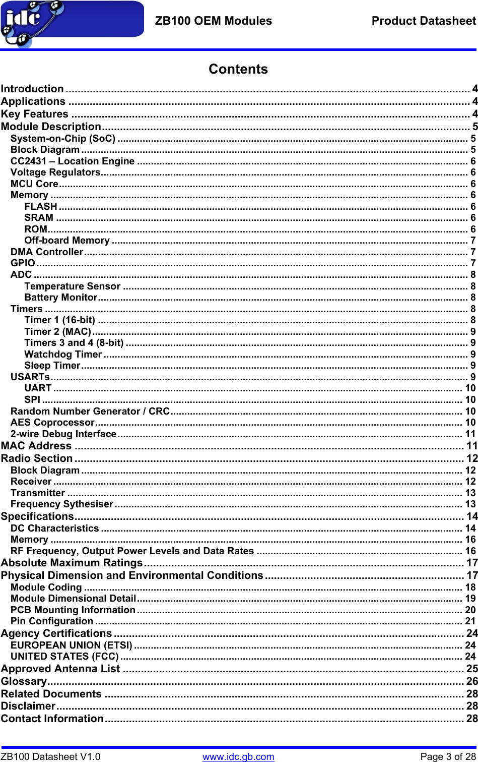
Voltage regulator Datasheet
Manual
Navigation menu
Upload a User Manual
Namespaces
Wiki Guide
HTML
PDF
Info
Views
User Manual
Discussion / Help
Navigation
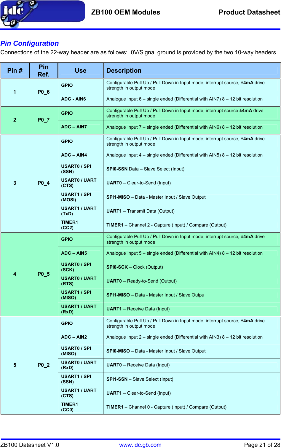
![ZB100 OEM Modules Product Datasheet ZB100 Datasheet V1.0 www.idc.gb.com Page 11 of 28 The AES coprocessor can add security to wired links (UART / SPI) but primarily is intended for the wireless link. AES encryption is performed on blocks of data (128-bit wide), prior to transmitting a packet payload over the radio, and AES decryption after receiving a payload packet. Ref [4] for further detail on AES operation. 2-wire Debug Interface The Debug Interface operates a proprietry 2-wire serial interface used for in-circuit debugging. Through this interface it is possible to erase and write (program) the FLASH memory, and debug by controlled program execution (stop/start, single stepping, breakpoints etc.). The 2-wire debug interface shares with two GPIO port pins, and the debug mode is entered by a specific operation of the debug clock in conjunction with the precessor RESETn pin. When not in debug mode, the port pins revert back to standard general purpose IO pins. The following details are for providing a programming interface for use with the Texas Instruments CC2430 Development Kit – CC2430DK. This uses a 10-way ribbon interface for programming and debugging the SoC. In addition, this example interface can also provide a single SPI port. Alternatively Radio Test signals can be configured to be outputs on the Port Pins P1_4 to P1_7 as given below. MAC Address The MAC address can be either hard-coded into FLASH, or take the address from the on-board 1-wire serial device connected to the CC2430/31 Port P2_0. This device can be either a generic 24-bit serial number, or a user specific EUI-64 global identifier whereby the first 24-bits provide the OUI, and the remaining 40-bits provide the serialisation. The IEEE assigned OUI for Intelligent Distributed Controls Limited is 00-1B-0A. OEMs may hardcode their own UID and serialisation or take the Intelligent Distributed Controls OUI as appropriate See Reference [6] for implimenting the 1-wire interface in software. MISOP1_70VRESETnSCLKP1_3+3.3VRESETnSoC PROGRAMMING DEBUG / FLASHSCLK0VP2_1P1_6P1_6SOCBox Header 2x512345678910P0_1P1_40VP0_3P2_1P1_4P2_2P0_2M11234567891011 1213 1415 1617 1819 2021 22RESETnP0_4P2_2HD212345678910P1_5P1_7P1_2Debug DC Debug DDP0_6MOSIP0_7P0_0Footprint of IDC00008S ModuleRESETn0VP1_1VregP0_5Debug DC0VMISOP1_5+3.3V3V3CSnVunreg Debug DDP1_0HD312345678910MOSIINTERFACEZB100 Module Radio Test Signals P1_4 – FIFO (One or more bytes in receive FIFO) P1_5 – FIFOP (Unread receive FIFO bytes overflow) P1_6 – SFD (Start of Frame Delimiter) P1_7 – CCA (Clear Channel Assessment)](https://usermanual.wiki/Intelligent-Distributed-Controls/ZB100.Manual/User-Guide-986390-Page-11.png)
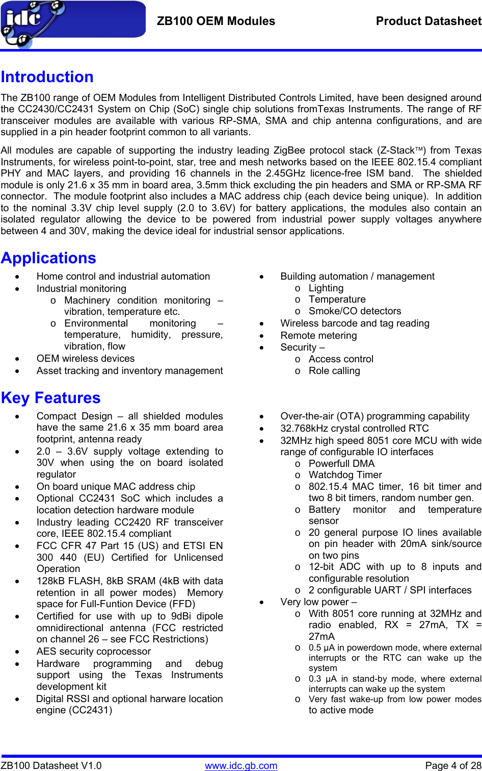
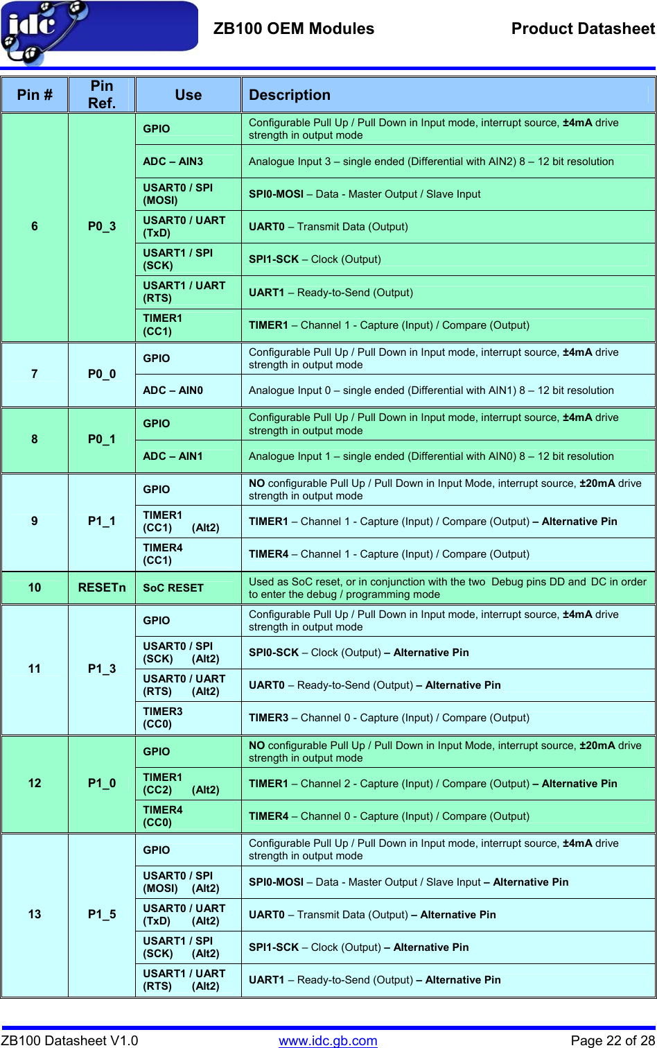
![ZB100 OEM Modules Product Datasheet ZB100 Datasheet V1.0 www.idc.gb.com Page 12 of 28 Radio Section The radio core is based on the industry standard Chipcon/TI CC2420 transceiver. The IEEE 802.15.4 compliant radio is shown below in a simplified block diagram. Operation of the radio is configured through a set of RF registers and controlled through a set of command strobes (single byte instructions) which control the functionality of the radio. E.g. enable frequency synthesiser, enable receive mode, enable transmit mode etc. The RF registers also provide status information from the radio. All command strobes from the CPU to the radio pass through the CSMA/CA Strobe Processor Refer to [1] for more detailed description of the radio operation. Block Diagram Receiver The CC2430/31 SoC contains a low-IF receiver. The received RF signal is amplifier by a low-noise amplifer (LNA) and down-converted in quadrature to the 2MHz intermediate frequency. The complex I/Q signal is then bandpass filtered and amplified with a variable gain amplifier. The gain of the amplifier is digitally controlled, and the AGC feedback loop ensures that the ADC operates inside its dynamic range. The signal is digitised by the ADCs. The AGC, final channel filtering, demodulation, de-spreading, symbol-correlation and byte synchronisation are performed digitally. IRQ handling presents an interrupt when a start of frame delimiter has been detected. A 128 byte receive FIFO is provided to buffer the received data. The firmware may read the receive FIFO through the SFR interface, ideally by DMA transfer into CPU memory. The receive FIFO is provided with overflow detection, informing the CPU via interrupt. The CRC is verified in hardware, and the RSSI and correlation values are appended to the received frame. The clear channel assessment, CCA, is available through an interrupt in receive mode. AES decryption (if adopted) is then handled by the CPU and AES coprocessor independent from the radio. LNA PA ΣTX/RX SWITCH Power Control TX POWER CONTROL AUTOMATIC GAIN CONTROLADCADCDACDAC090FREQUENCYSYNTHESISER~ DIGITAL DEMODULATOR -Digital RSSI -Gain Control -Image Suppression -Channel Filtering -Demodulation -Frame synchronisation DIGITAL MODULATOR -Data spreading -Modulation CONTROL LOGIC RADIO DATA INTERFACE FFCTRL IRQ HANDLING SFR bus RADIO REGISTER BANK CSMA/CA STROBE PROCESSORRegister Bus ≡ CC2420 Transceiver](https://usermanual.wiki/Intelligent-Distributed-Controls/ZB100.Manual/User-Guide-986390-Page-12.png)
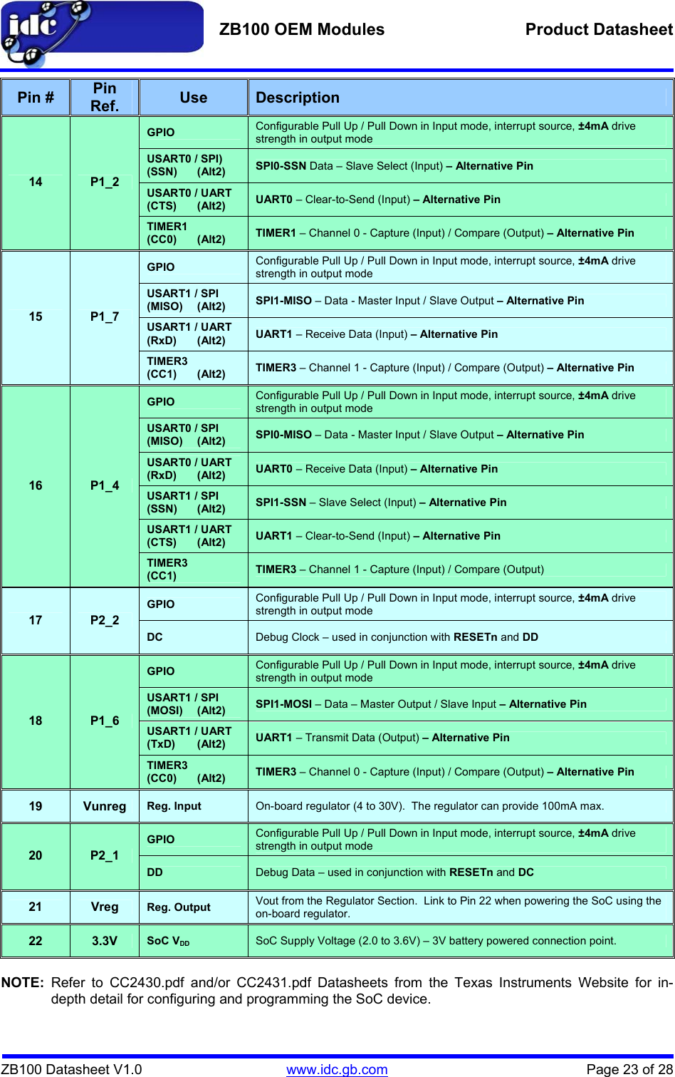
![ZB100 OEM Modules Product Datasheet ZB100 Datasheet V1.0 www.idc.gb.com Page 16 of 28 Memory Parameter Min Typ Max Unit Condition/Note FLASH Memory 128 kbyte 64 pages of 2kbyte each Page erase time 20 ms Chip mass erase time 200 ms Write time 20 µs Per 4 bytes Data Retention 100 years At room temperature Program erase/write 1000 cycles endurance SRAM 4096 bytes Data retention in all power modes SRAM 4096 bytes Data retention in power modes 0 (active) and 1. MAC / Serial Chip 64 bit ROM accessed through 1-wire interface RF Frequency, Output Power Levels and Data Rates Parameter Min Typ Max Unit Condition/Note RF Frequency Range 2400 2483.5 MHz Programmable in 1 MHz steps, 5 MHz between channels for compliance with [1]. No. of channels 16 ** – See RF channel table. Channel Spacing 5 Mhz ** Radio bit rate 250 kbps ** Radio Chip Rate 2.0 MChip/s ** Receiver Sensitivity -92 dBm PER = 1%, as specified by [1]. Nominal Output power 0 dBm Delivered to a single ended 50 Ω load through a balun and output power control set to 0x5F (TXCTRLL register). Programmable output power range 26 dBm The output power is programmable in 16 steps from typically -25.2 to +0.6 dBm. Antenna nominal RX / TX impedance 50 Ω The RF channels and associated frequencies defined by the IEEE 802.15.4 standard are as follows: [1] IEEE std. 802.15.4 - 2003: Wireless Medium Access Control (MAC) and Physical Layer (PHY) specifications for Low Rate Wireless Personal Area Networks (LR-WPANs).RF Channel Frequency RF Channel Frequency RF Channel Frequency 11 2405 MHz 17 2435 MHz 23 2465 MHz 12 2410 MHz 18 2440 MHz 24 2470 MHz 13 2415 MHz 19 2445 MHz 25 2475 MHz 14 2420 MHz 20 2450 MHz 26 2480 MHz 15 2425 MHz 21 2455 MHz 16 2430 MHz 22 2460 MHz](https://usermanual.wiki/Intelligent-Distributed-Controls/ZB100.Manual/User-Guide-986390-Page-16.png)
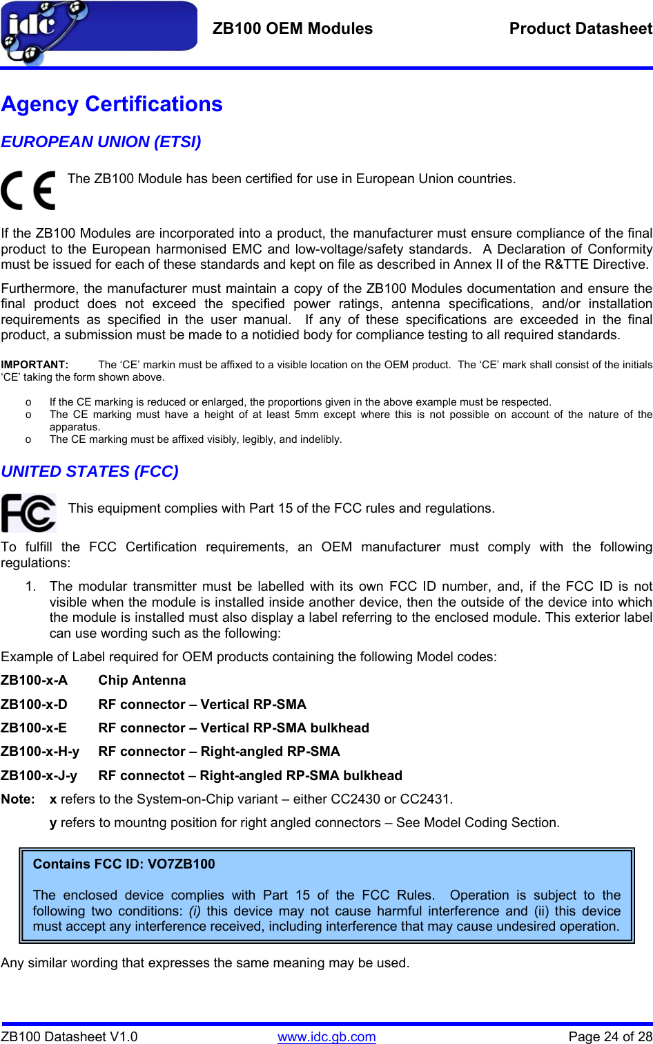
![ZB100 OEM Modules Product Datasheet ZB100 Datasheet V1.0 www.idc.gb.com Page 17 of 28 Absolute Maximum Ratings Parameter Min Typ Max Unit Condition/Note Supply Voltage VDD -0.3 3.9 V Header Pin 22 – referenced to 0V. Supply Voltage Vunreg V Header Pin 19 – referenced to 0V. Voltage on any digital IO pin -0.3 VDD+0.3 max 3.9 V Input RF Level 10 dBm Storage temp -50 +150 ºC Device not programmed. Caution!! ZB100 Modules are ESD sensitive devices. Precautions should be taken when handling the device in order to prevent permanent damage. Physical Dimension and Environmental Conditions All modules are RoHS Compliant in construction. Parameter Value Notes / Module Codes Size – board profile 21.6 x 35 mm Excludes over-hang of SMA or RP-SMA RF connectors. See dimensional drawings for RF connector positions and board overhang etc. Module height 3.5 mm Board and RF shield combined - excluding pin headers. 4.8 mm ZB100-0-A; ZB100-1-A 12.3 mm ZB100-0-B; ZB100-0-D; ZB100-1-B; ZB100-1-D 16.3 mm ZB100-0-C; ZB100-0-E; ZB100-1-C; ZB100-1-E 12.3 mm ZB100-0-F-z; ZB100-0-H-z; ZB100-1-F-z; ZB100-1-H-z Total height above OEM daughter board (See Dimensional drawings) 12.3 mm ZB100-0-G-z; ZB100-0-J-z; ZB100-1-G-z; ZB100-1-J-z 6 g ZB100-0-A; ZB100-1-A 8 g ZB100-0-B; ZB100-0-D; ZB100-1-B; ZB100-1-D 10 g ZB100-0-C; ZB100-0-E; ZB100-1-C; ZB100-1-E 8 g ZB100-0-F-z; ZB100-0-H-z; ZB100-1-F-z; ZB100-1-H-z Weight (approx.) 10 g ZB100-0-G-z; ZB100-0-J-z; ZB100-1-G-z; ZB100-1-J-z Operating Temperature -20ºC to +70ºC -40ºC to +85ºC Storage and Operational with minor degradation of clock stability / accuracy. Operating Relative Humidity 80% RH For in-depth specifications please refer to the Related Documents - [1].](https://usermanual.wiki/Intelligent-Distributed-Controls/ZB100.Manual/User-Guide-986390-Page-17.png)
![ZB100 OEM Modules Product Datasheet ZB100 Datasheet V1.0 www.idc.gb.com Page 28 of 28 Related Documents [1] Chipcon Products fromTexas Instruments CC2430 – A True System-on-Chip solution for 2.4GHz IEEE 802.15.4 / ZigBee CC2430 Data Sheet (Rev. 2.1) SWRS036F [2] Chipcon Products fromTexas Instruments CC2431 – System-on-Chip for 2.4 GHz ZigBee®/ IEEE 802.15.4 with Location Engine CC2431 Data Sheet (Rev. 2.01) SWRS034B [3] Chipcon Products fromTexas Instruments – Application Note AN042 – CC2431 Location Engine Application Note AN042 (Rev. 1.0) SWRA095 [4] Design Note DN108 – Using AES Encryption in CC111xFx, CC243x, and CC251xFx SWRA172A [5] CC1110DK/ CC2430DK/CC2510DK Development Kit - User Manual - Rev. 1.5 SWRU039 [6] Dallas/Maxim – 1-wire Communication Through Software – App Note 126 Disclaimer Intelligent Distributed Controls Limited believes that at the time of issue, all information contained herein to be accurate. Intelligent Distributed Controls Limited reserves the right to make changes to this product or documentation without prior notice. Latest available revisions shall be provided on the Website. Contact Information Intelligent Distributed Controls Limited Suite 6 Keynes House Chester Park Alfreton Road Derby DE21 4AS United Kingdom Tel: +44(0)1332 604030 Fax: +44(0)1332 604031 E-mail: sales @idc.gb.com Website: www.idc.gb.com Office Hours: 9:00am - 5:00pm GMT](https://usermanual.wiki/Intelligent-Distributed-Controls/ZB100.Manual/User-Guide-986390-Page-28.png)