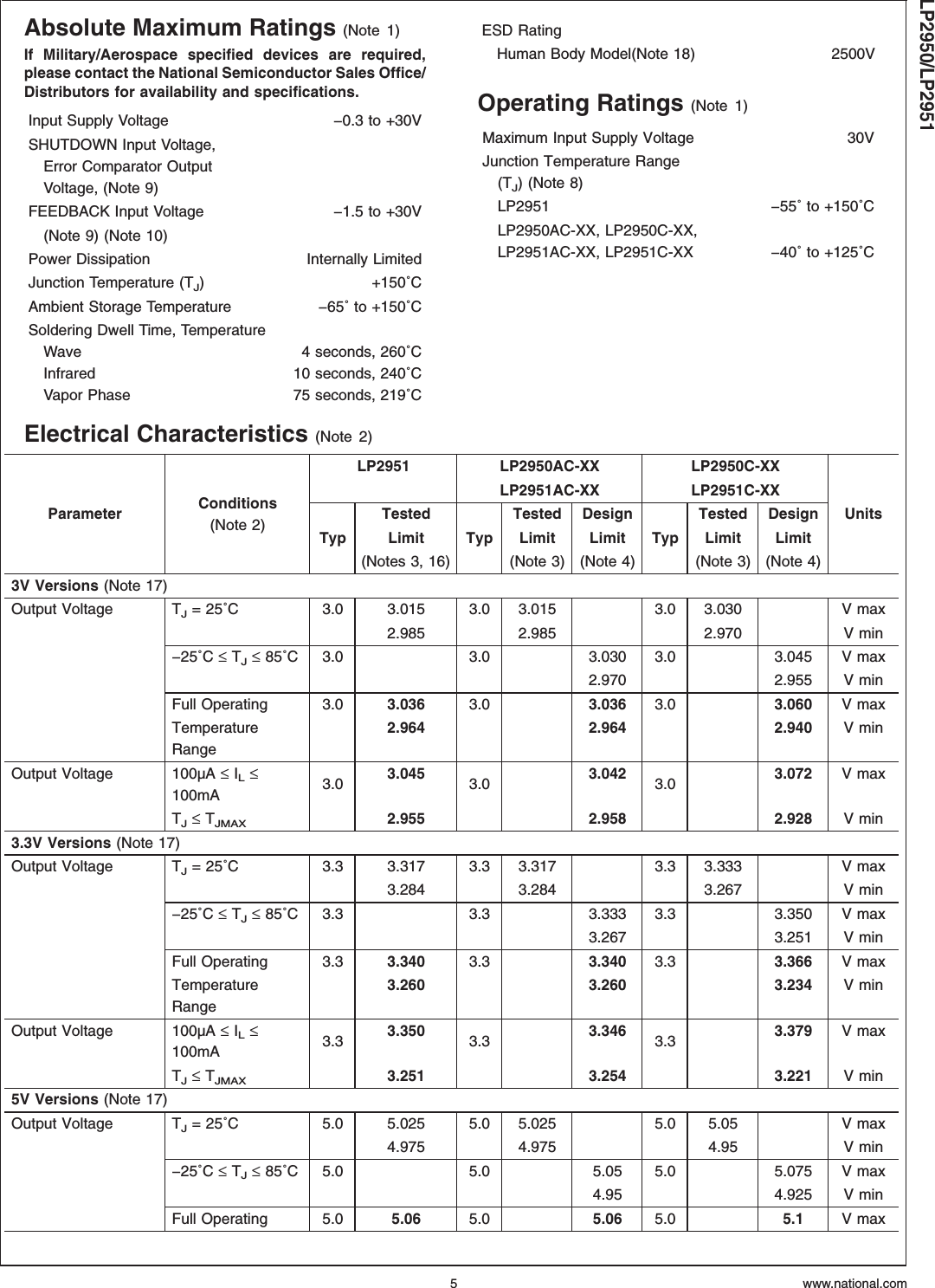
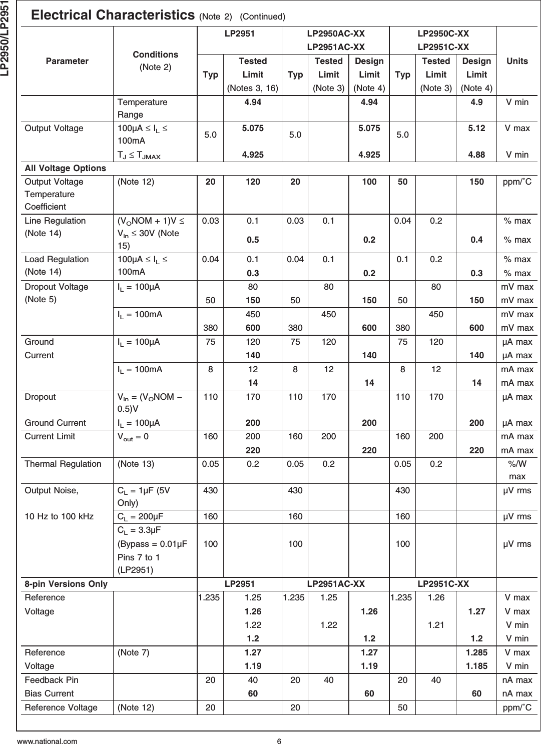
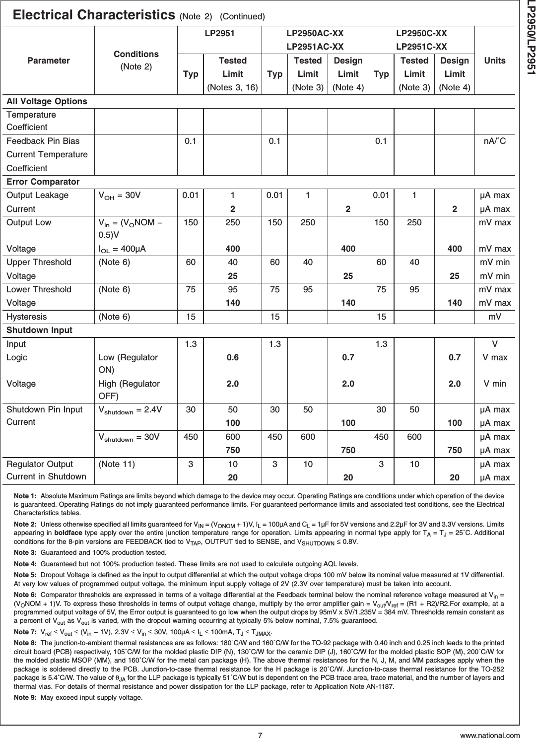
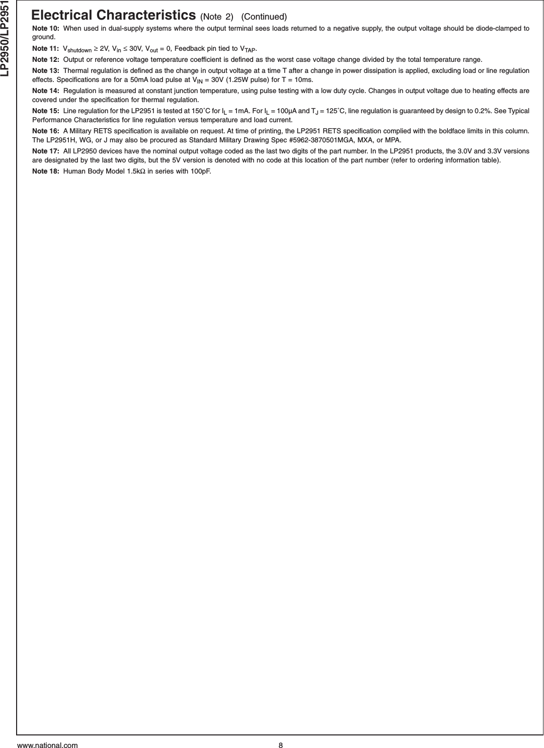
Intelligent Distributed Controls ZB100 ZB100 ZigBee Module User Manual Voltage regulator Datasheet
Intelligent Distributed Controls Limited ZB100 ZigBee Module Voltage regulator Datasheet
Contents
- 1. Manual
- 2. Voltage regulator Datasheet
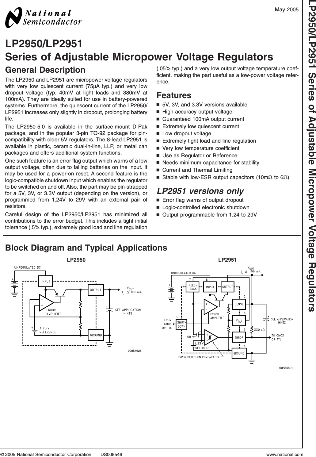
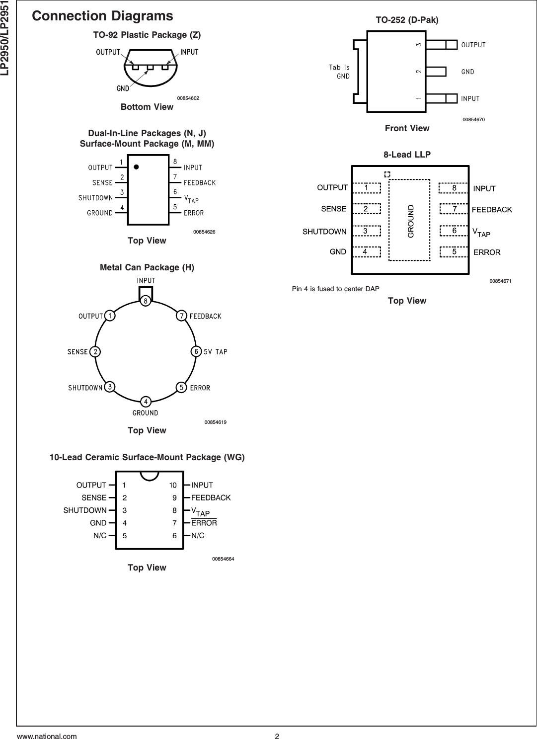
Voltage regulator Datasheet