M2Communication MA903A1 Wireless AP Module_9 series User Manual MA903A1 FCC 20151021
M2Communication Inc. Wireless AP Module_9 series MA903A1 FCC 20151021
UserManual.wiki
>
M2Communication
>
MA903A1 User Manual
OEM Manual
Navigation menu
Upload a User Manual
Namespaces
Wiki Guide
HTML
PDF
Info
Views
User Manual
Discussion / Help
Navigation
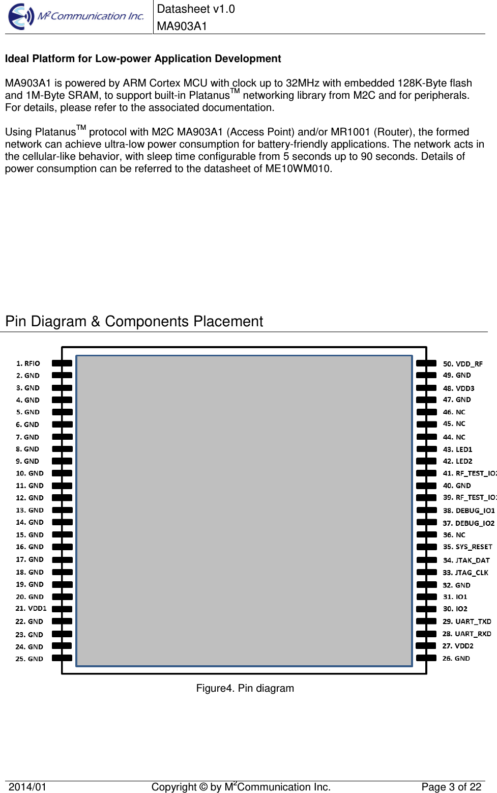
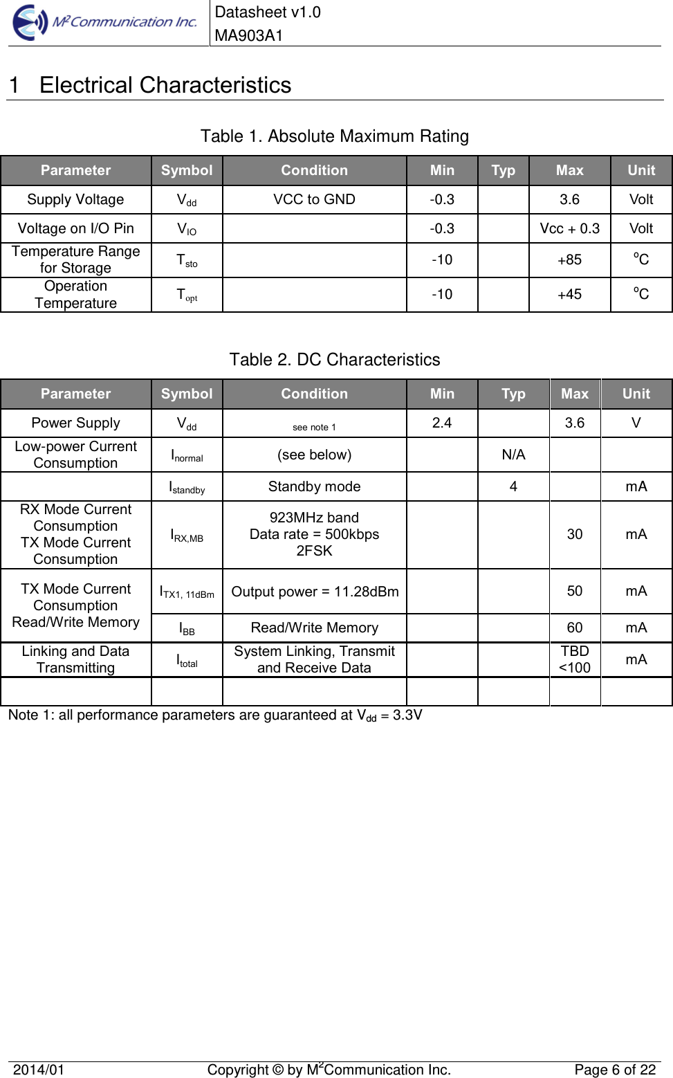
![Datasheet v1.0 MA903A1 2014/01 Copyright © by M2Communication Inc. Page 9 of 22 2 Pin Out All VDDs are rated from 2.4V to 3.6V. Pin # Pin Name Description Type[1] I/O/PWR 1 RFIO RF Signal 50 ohm IO RF 2~20, 22~26, 32, 40, 47, 49 GND Board ground G 0 21 VDD1 Module Power Input. 2.4V~3.6V VDD1+VDD2+VDD3+VDD_RF 150mA Requirement P PWR 27 VDD2 Module Power Input. 2.4V~3.6V VDD1+VDD2+VDD3+VDD_RF 150mA Requirement P PWR 28 UART_RXD UART_RXD, Baud Rate = 460.8kbps D/A IO 29 UART_TXD UART_TXD, Baud Rate = 460.8kbps D/A IO 30 IO2 GPIO D IO 31 IO1 GPIO D IO 33 JTAG_CLK ICE CLK (debugger) D I 34 JTAG_DAT ICE DATA IN (debugger) D IO 35 SYS_RESET External reset input, No need RC Delay [2] SYS SYS 36, 44~46 NC No Connection 37 DEBUG_IO2 Debug UART_TXD, No connection D O 38 DEBUG_IO1 Debug UART_RXD, No connection D I 39 RF_TEST_IO1 RF Test Pin Data_Out, No connection D O 41 RF_TEST_IO2 RF Test Pin CLK_Out, No connection D O 42 LED2 LED Index, Driver current 3mA D IO 43 LED1 LED Index, Driver current 3mA D IO 48 VDD3 Module Power Input. 2.4V~3.6V VDD1+VDD2+VDD3+VDD_RF 150mA Requirement P PWR 50 VDD_RF Module Power Input. 2.4V~3.6V VDD1+VDD2+VDD3+VDD_RF 150mA Requirement P PWR [1] D=digital, A=analog, P=power, G=ground [2] Set this pin low reset chip to initial state, with internal pull-up [3] External interrupt input](https://usermanual.wiki/M2Communication/MA903A1/User-Guide-2793624-Page-9.png)