Murata Electronics North America 2100 Class 1 Bluetooth compliant device User Manual SN2100 Datasheet
Murata Electronics North America Class 1 Bluetooth compliant device SN2100 Datasheet
UserManual.wiki
>
Murata Electronics North America
>
2100 User Manual
Users Manual
Navigation menu
Upload a User Manual
Namespaces
Wiki Guide
HTML
PDF
Info
Views
User Manual
Discussion / Help
Navigation
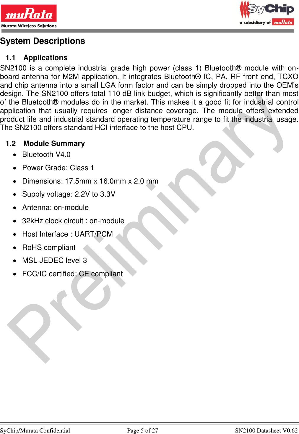
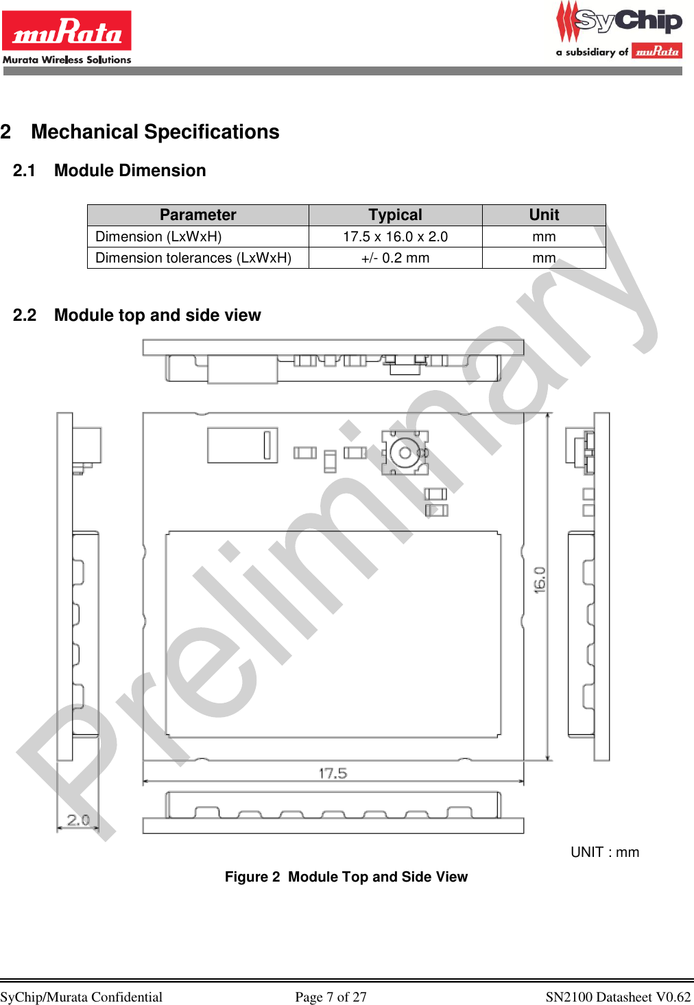
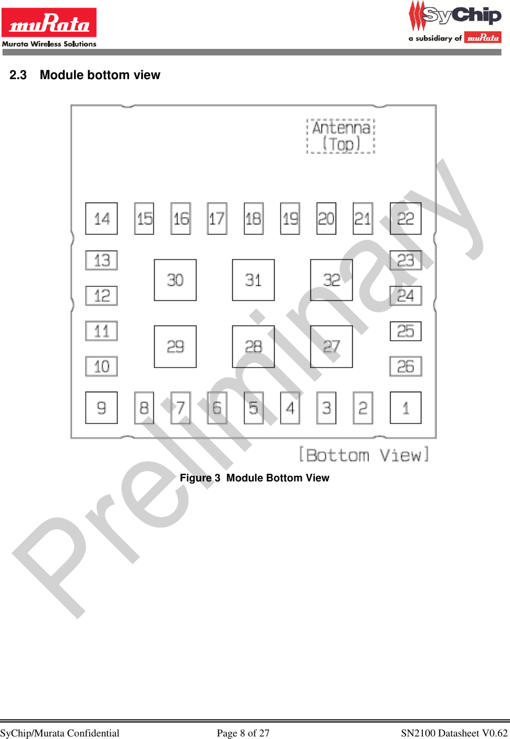
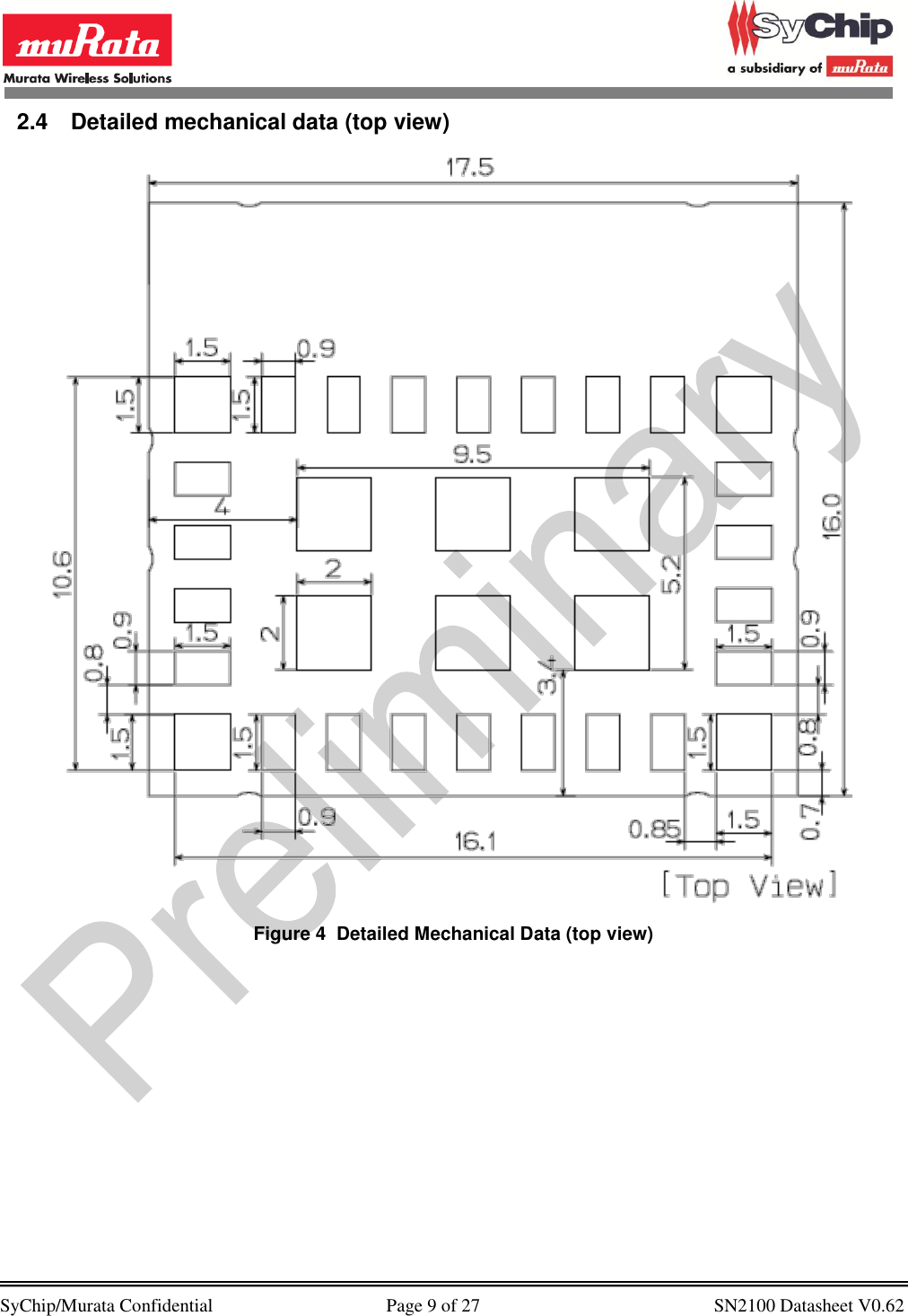
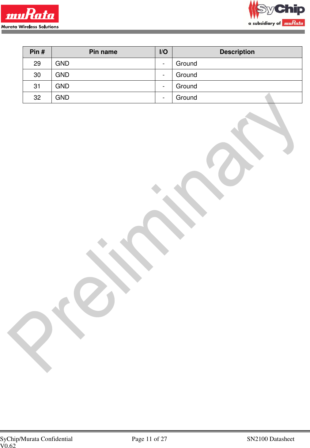
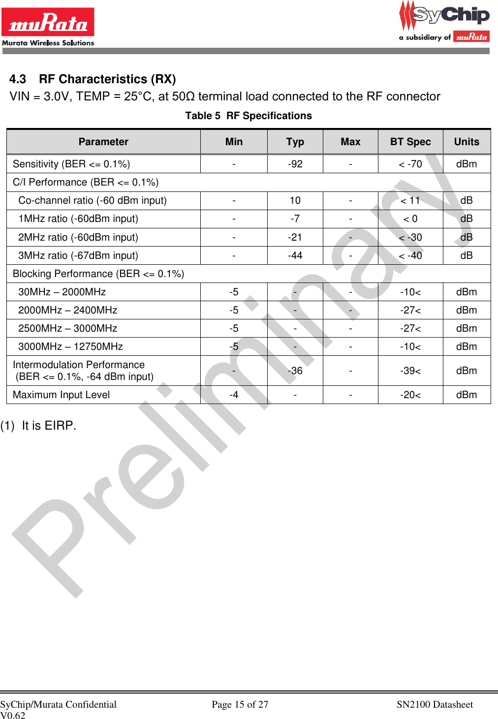
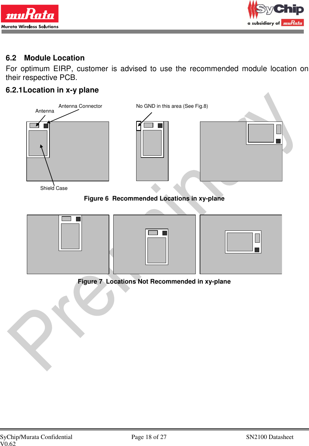
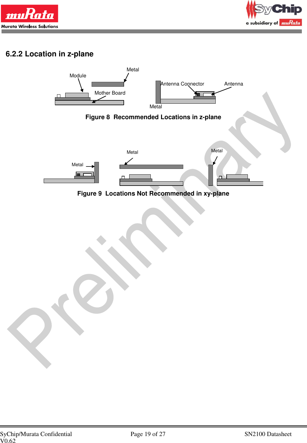
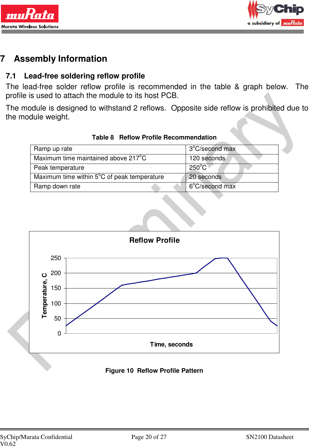
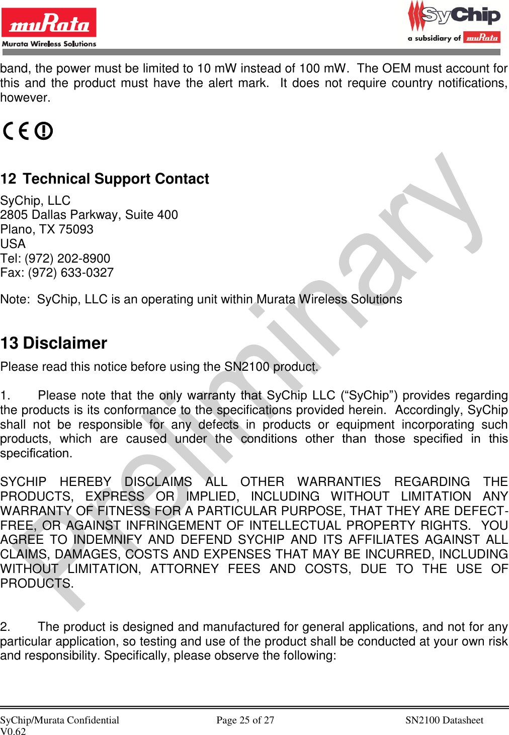
![SyChip/Murata Confidential Page 13 of 27 SN2100 Datasheet V0.62 4 RF Specifications 4.1 Bluetooth Specification Parameter Contents Bluetooth Specification Ver.4.0 Channel Spacing 1 MHz The number of channel 79 Power Class 1 4.2 RF Characteristics (TX) VIN = 3.0V, TEMP = 25°C, at 50Ω terminal load connected to the RF connector Table 4 RF Specifications Parameter Min Typ Max BT Spec Units Output Power - 18 - 20(1) dBm Operation Frequency range (RX/TX) 2402 - 2480 - MHz -20 dB bandwidth - 0.928 - 1 MHz Adjacent Channel Power [M-N] = 2 - -40 - <-20 dBm [M-N] >= 3 - -43 - <-40 dBm Modulation Characteristics Modulation delta f1 avg - 159 - 140< <175 kHz Modulation delta f2 max - 136 - 115< kHz Modulation delta f2 avg/delta f1 avg - 0.9 - 0.8< - Initial Carrier Frequency Tolerance - -2 - -75< <75 kHz Carrier Frequency Drift 1 slot -25 2 - -25< <25 kHz 3 slot -40 1 - -40< <40 kHz 5 slot -40 1 - -40< <40 kHz Maximum drift rate -20 0.5 - -20< <20 kHz/50 us Out of Band Spurious Emissions 30 – 1000 MHz (Operation Mode) - -50 - <-36 dBm 1000 – 12750 MHz (Operation Mode) - -52 - <-30 dBm 1800 – 1900 MHz (Operation Mode) - -54 - <-47 dBm](https://usermanual.wiki/Murata-Electronics-North-America/2100/User-Guide-1690087-Page-13.png)