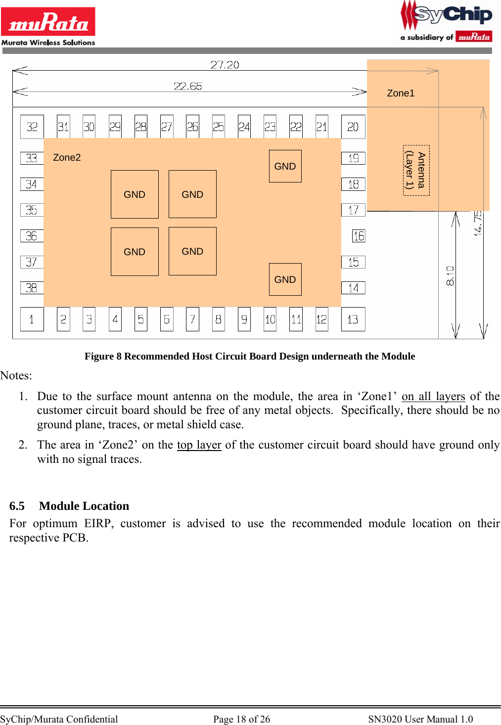
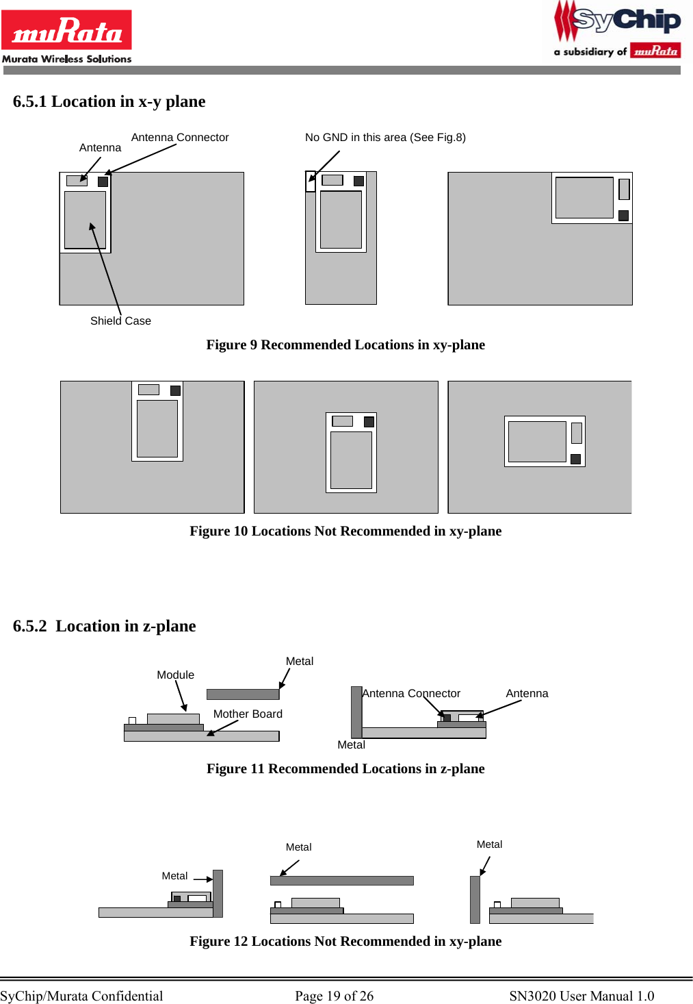
Murata Electronics North America 3020 SYCHIP SN3020 IEEE802.15.4/ZIGBEE SMART ENERGY MODULE User Manual SN3020 Datasheet Manual v1 0
Murata Electronics North America SYCHIP SN3020 IEEE802.15.4/ZIGBEE SMART ENERGY MODULE SN3020 Datasheet Manual v1 0
Users Manual
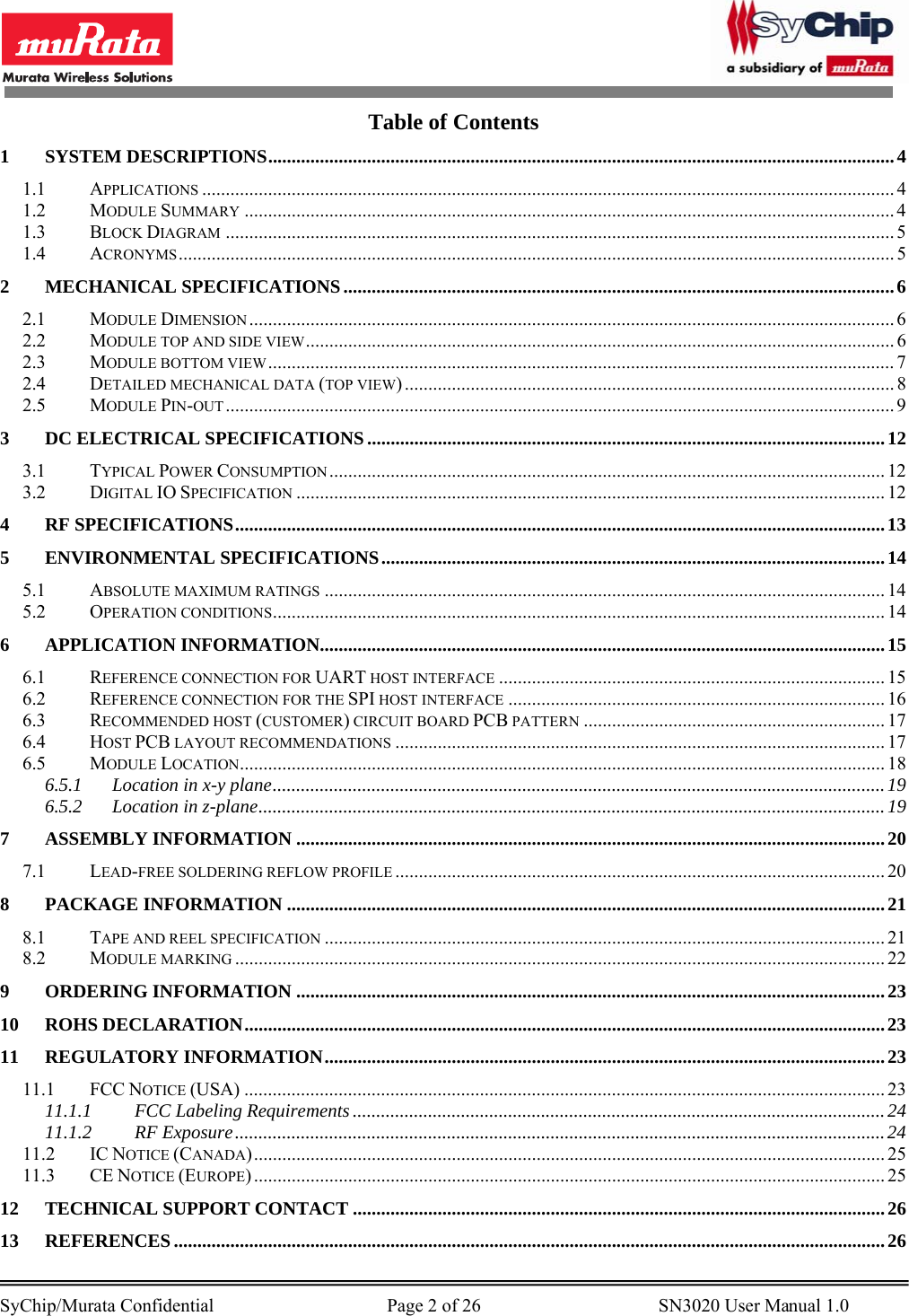
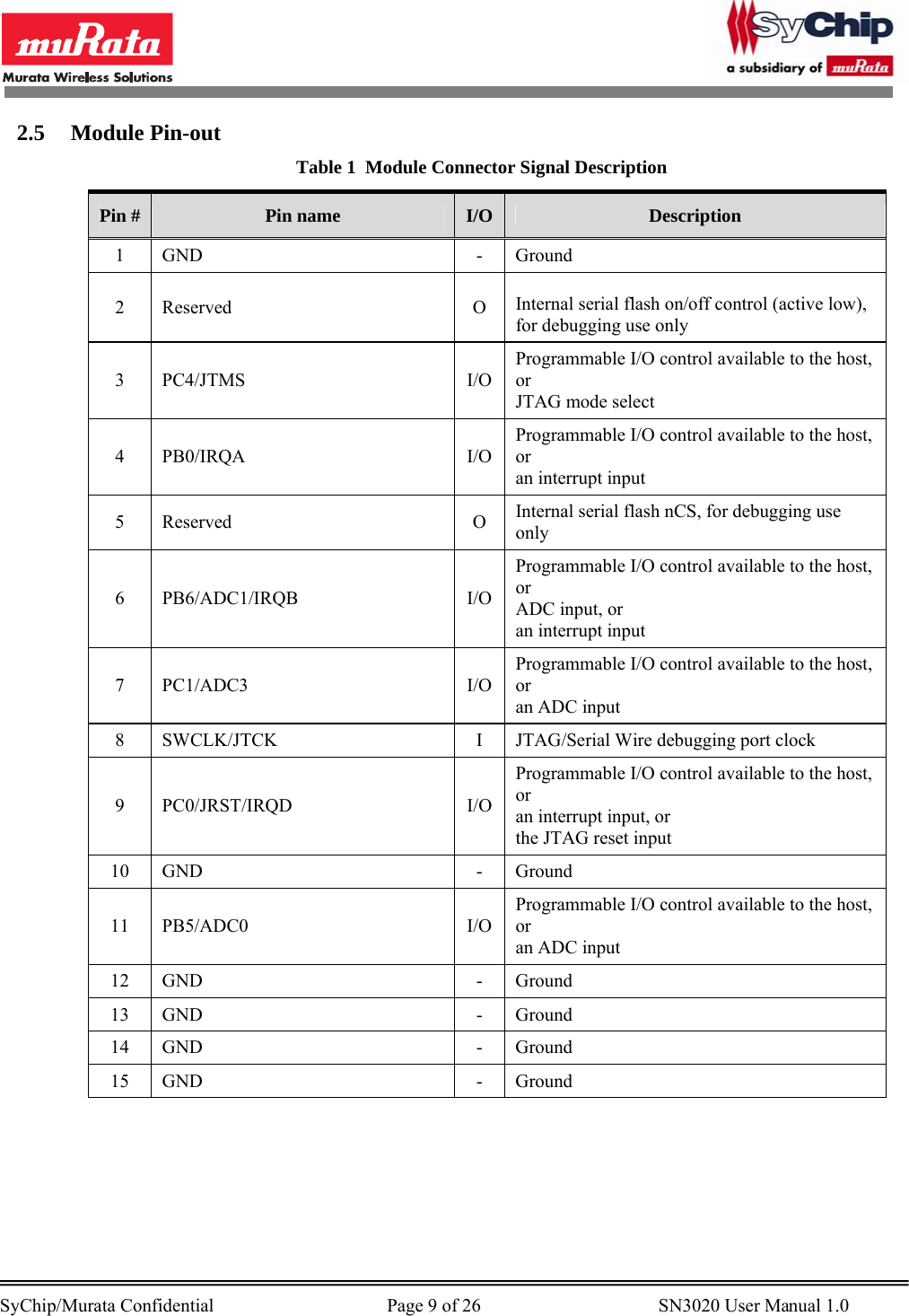
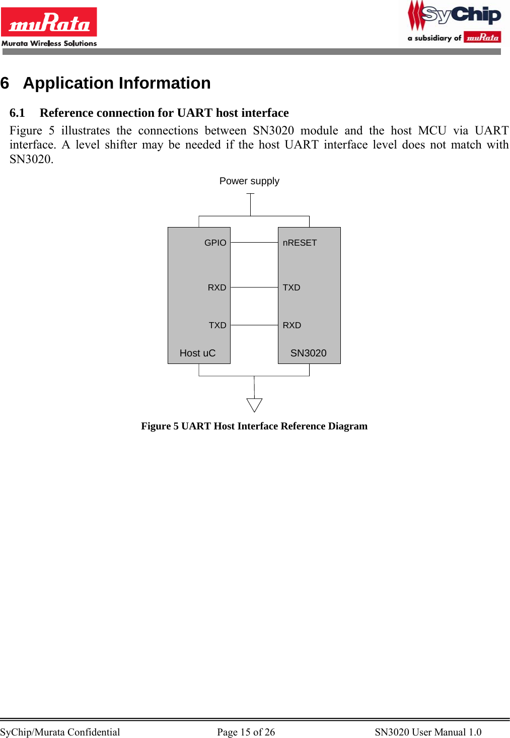
![SyChip/Murata Confidential Page 13 of 26 SN3020 User Manual 1.0 High Schmitt switching threshold Schmitt input threshold going from low to high VSWIH 0.62 x VCC 0.8 x VCC V Output voltage for logic 0 IOL = 4mA (8mA) for standard (high current) pads VOL 0 0.18 x VCC V Output voltage for logic 1 IOH = 4mA (8mA)for standard (high current) pads VOH 0.82 x VCC VCC V Output Source Current Standard current pad IOHS 4 mA Output Sink current Standard current pad IOLS 4 mA Output Source Current High current pad IOHH 8 mA Output Sink current High current pad IOLH 8 mA Total output current IOH + IOL 40 mA 4 RF Specifications VCC = 3.0V, TAMB = 25°C, NORMAL MODE measured at 50Ω terminal load connected to the RF connector Table 4 RF Specifications Parameter Min Typ Max Units Frequency range 2400 2500 MHz Receiver sensitivity -103 dBm Maximum input signal level -20 dBm Transmitter power at the maximum setting 2 20 dBm Adjacent channel rejection 24 dB Alternate channel rejection 42 dB Carrier frequency error -40 +40 ppm 2 Ember RF output power programmed to -12 by emberSetRadioPower [2] or equivalent under NORMAL mode](https://usermanual.wiki/Murata-Electronics-North-America/3020/User-Guide-1422893-Page-13.png)
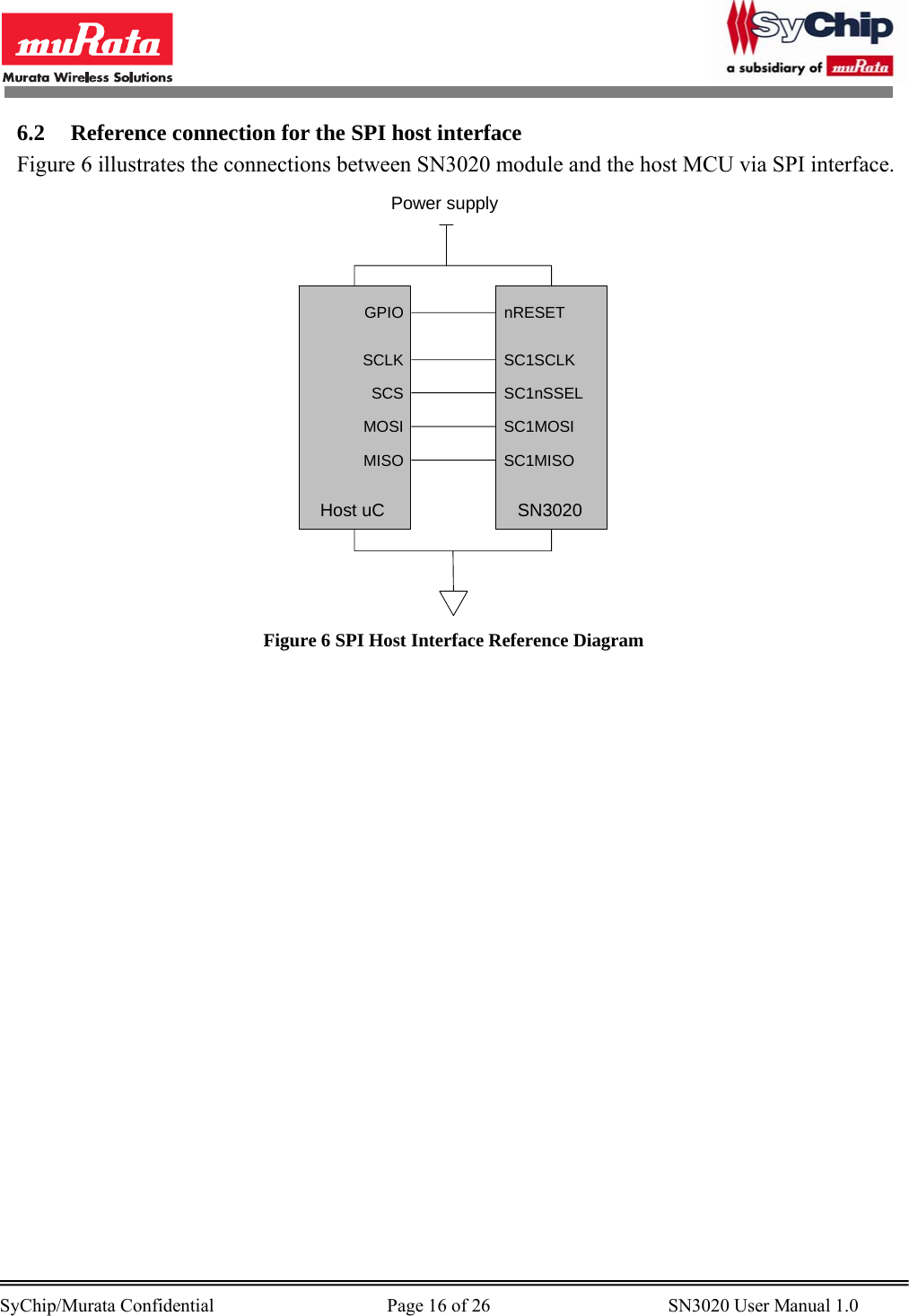
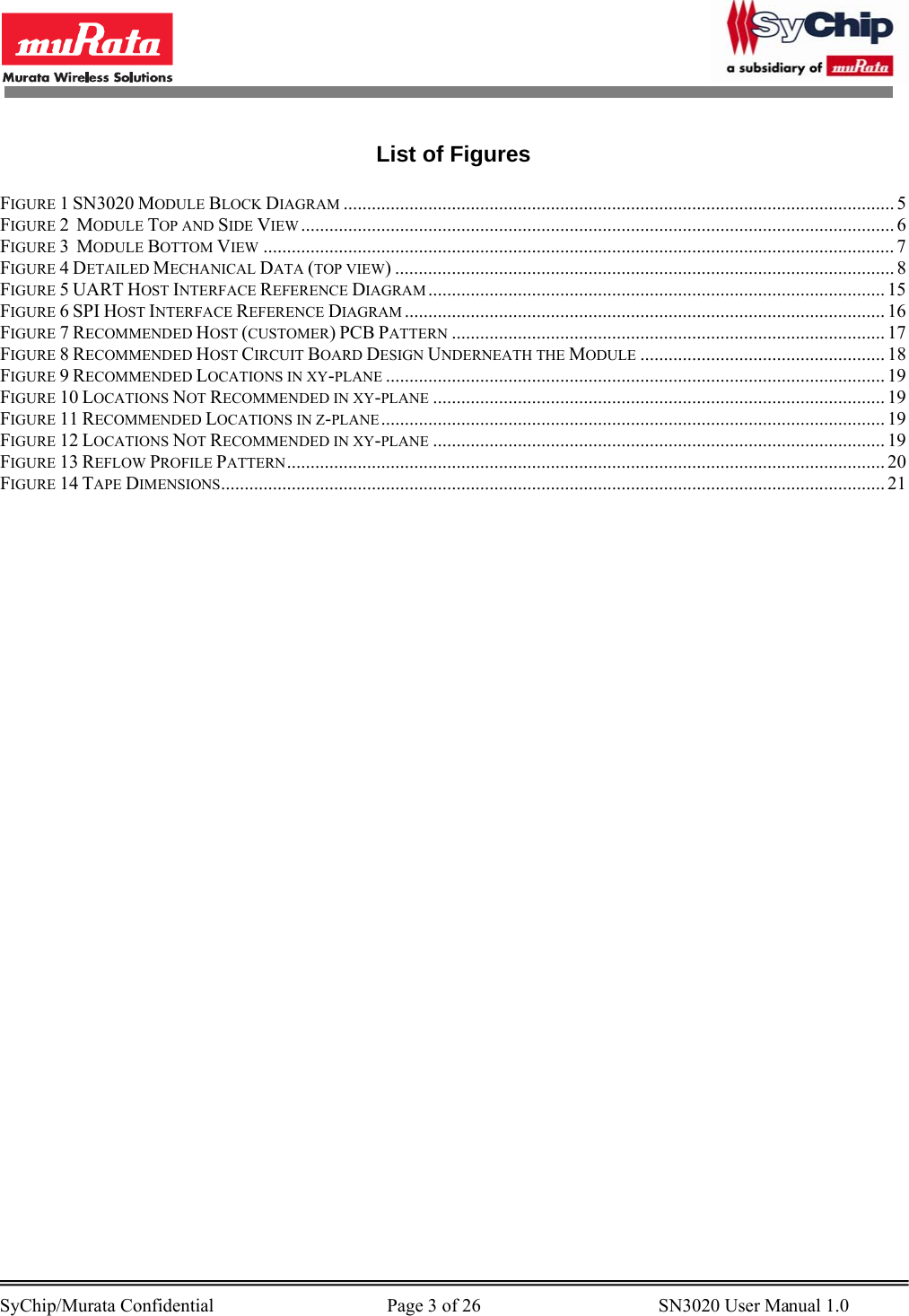
![SyChip/Murata Confidential Page 24 of 26 SN3020 User Manual 1.0 This device using the integrated antenna has been tested to comply with FCC CFR Part 15. The device meets the requirements for modular transmitter approval as detailed in the FCC public notice DA00.1407.transmitter given the following considerations: • Maximum output power level for the channels as defined by IEEE 802.15.4 [1] must be set to the value below using emberSetRadioPower or equivalent under NORMAL mode as specified in [2]. o For channels 11 to 24, the value of -11 o For channel 25, the value of -17 o For channel 26, the value of -27 • Duty cycle of 67% allowed. • The firmware disables power out if the source voltage is greater than 3.4V. • VBATT must be between 2.4V – 3.4V. This equipment has been tested and found to comply with the limits for a Class B digital device, pursuant to Part 15 of the FCC Rules. These limits are designed to provide reasonable protection against harmful interference in a residential installation. This equipment generates, uses and can radiate radio frequency energy and, if not installed and used in accordance with the instructions, may cause harmful interference to radio communications. However, there is no guarantee that interference will not occur in a particular installation. If this equipment does cause harmful interference to radio or television reception, which can be determined by turning the equipment off and on, the user is encouraged to try to correct the interference by one or more of the following measures: reorient or relocate the receiving antenna, increase the separation between the equipment and receiver, connect the equipment into an outlet on a circuit different from that to which the receiver is connected, or consult the dealer or an experienced radio/TV technician for help. 11.1.1 FCC Labeling Requirements When integrating the SN3020 into a product the FCC labeling requirements must be met. This includes a clearly visible label on the outside of the finished product specifying the SN3020 FCC identifier (FCC ID:QPU3020) as well as the notice above. The exterior label can use wording such as “Contains Transmitter Module FCC ID:QPU3020” or “Contains FCC ID:QPU3020” although any similar wording that expresses the same meaning may be used. 11.1.2 RF Exposure This module has been certified for remote and base radio applications and is not intended to be operated within 20cm of the body. If the module will be used for portable applications, the device must undergo SAR testing. The following statement must be included as a CAUTION statement in manuals for the products to alert users on FCC RF exposure compliance: “WARNING: To satisfy FCC RF exposure requirements for mobile transmitting devices, a separation distance of 20cm or more should be maintained between the antenna of this device and persons during operation. To ensure compliance, operations at closer distances than this are not recommended.”](https://usermanual.wiki/Murata-Electronics-North-America/3020/User-Guide-1422893-Page-24.png)
![SyChip/Murata Confidential Page 26 of 26 SN3020 User Manual 1.0 12 Technical Support Contact SyChip, Inc 2805 Dallas Parkway, Suite 400 Plano, TX 75093 USA Tel: (972) 202-8900 Fax: (972) 633-0327 Note: SyChip, Inc is an operating unit within Murata Wireless Solutions 13 References [1] IEEE Standard 802.15.4 – 2003 Wireless Medium Access Control (MAC) and Physical Layer (PHY) Specifications for Low-Rate Wireless Personal Area Networks (LR-WPANs) [2] Ember, “EmberZNet API Reference: For the EM35x SoC Platform”, 120-3022-000G, October 28 2010](https://usermanual.wiki/Murata-Electronics-North-America/3020/User-Guide-1422893-Page-26.png)