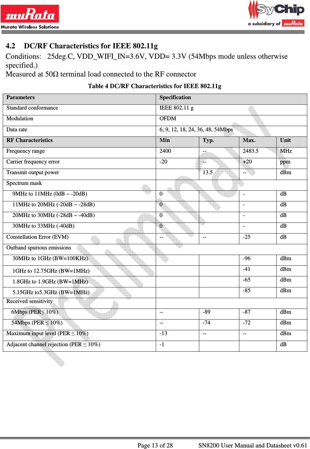
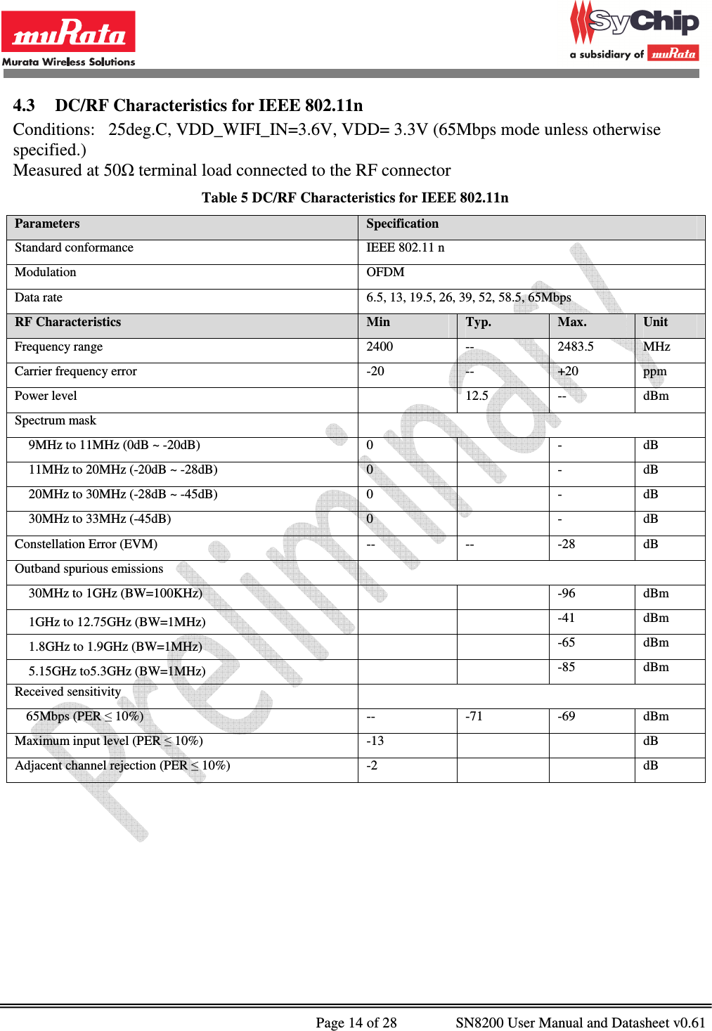
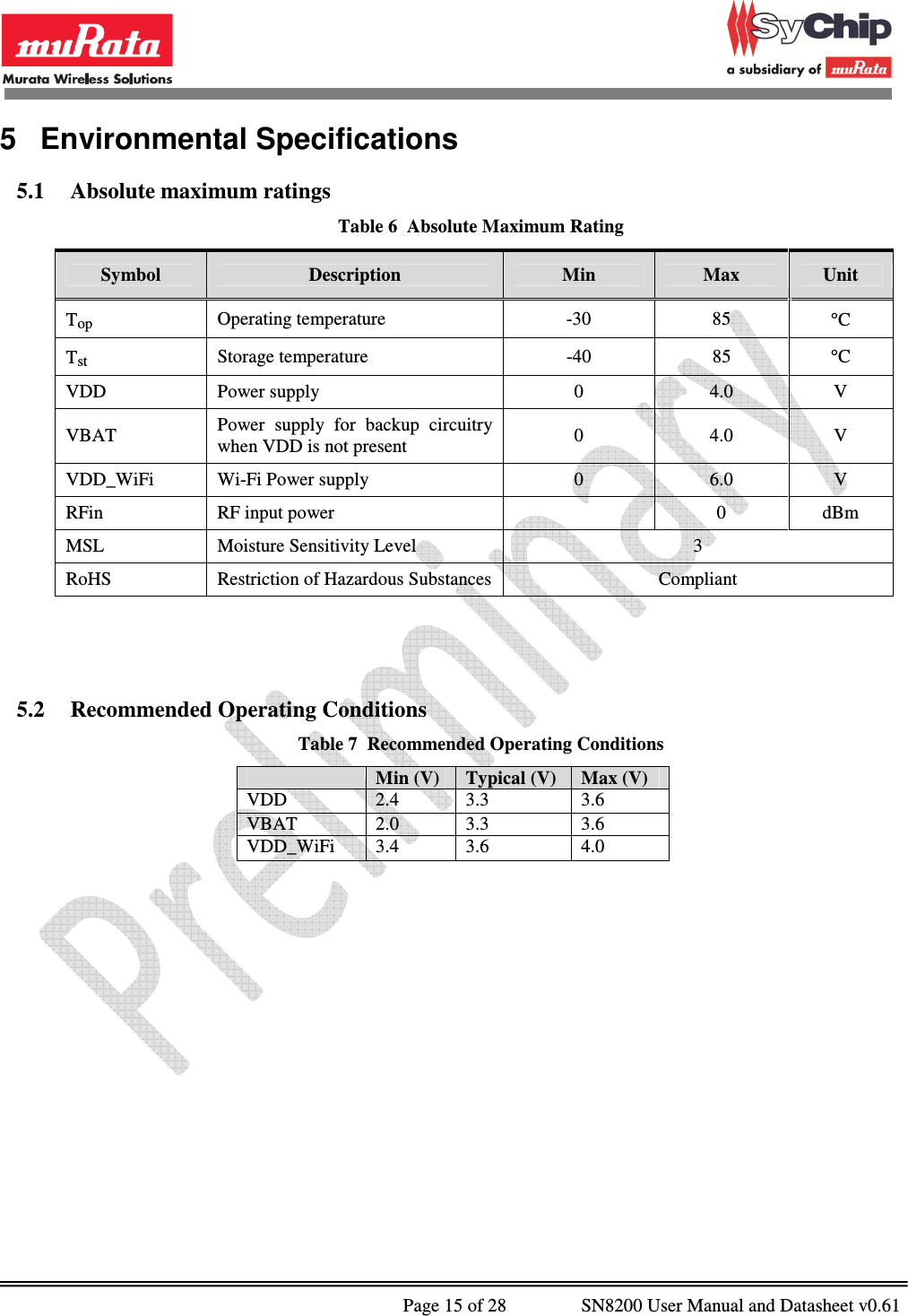
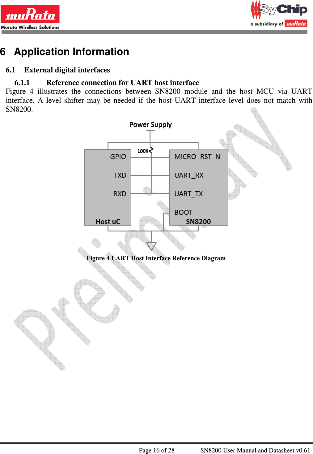
Murata Electronics North America 8200 Wi-Fi Network Controller Module User Manual
Murata Electronics North America Wi-Fi Network Controller Module
UserManual.wiki
>
Murata Electronics North America
>
8200 User Manual
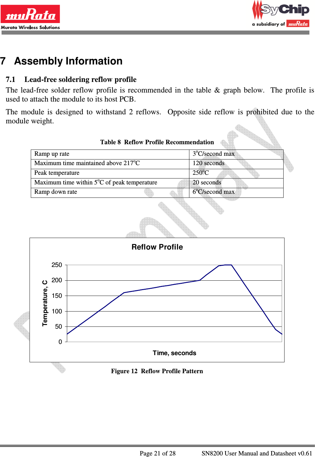
user manual
Navigation menu
Upload a User Manual
Namespaces
Wiki Guide
HTML
PDF
Info
Views
User Manual
Discussion / Help
Navigation