Murata Electronics North America DRWLS1271L DR-WLS1271L-102 User Manual
Murata Electronics North America DR-WLS1271L-102
UserManual.wiki
>
Murata Electronics North America
>
DRWLS1271L User Manual
User Manual
Navigation menu
Upload a User Manual
Namespaces
Wiki Guide
HTML
PDF
Info
Views
User Manual
Discussion / Help
Navigation
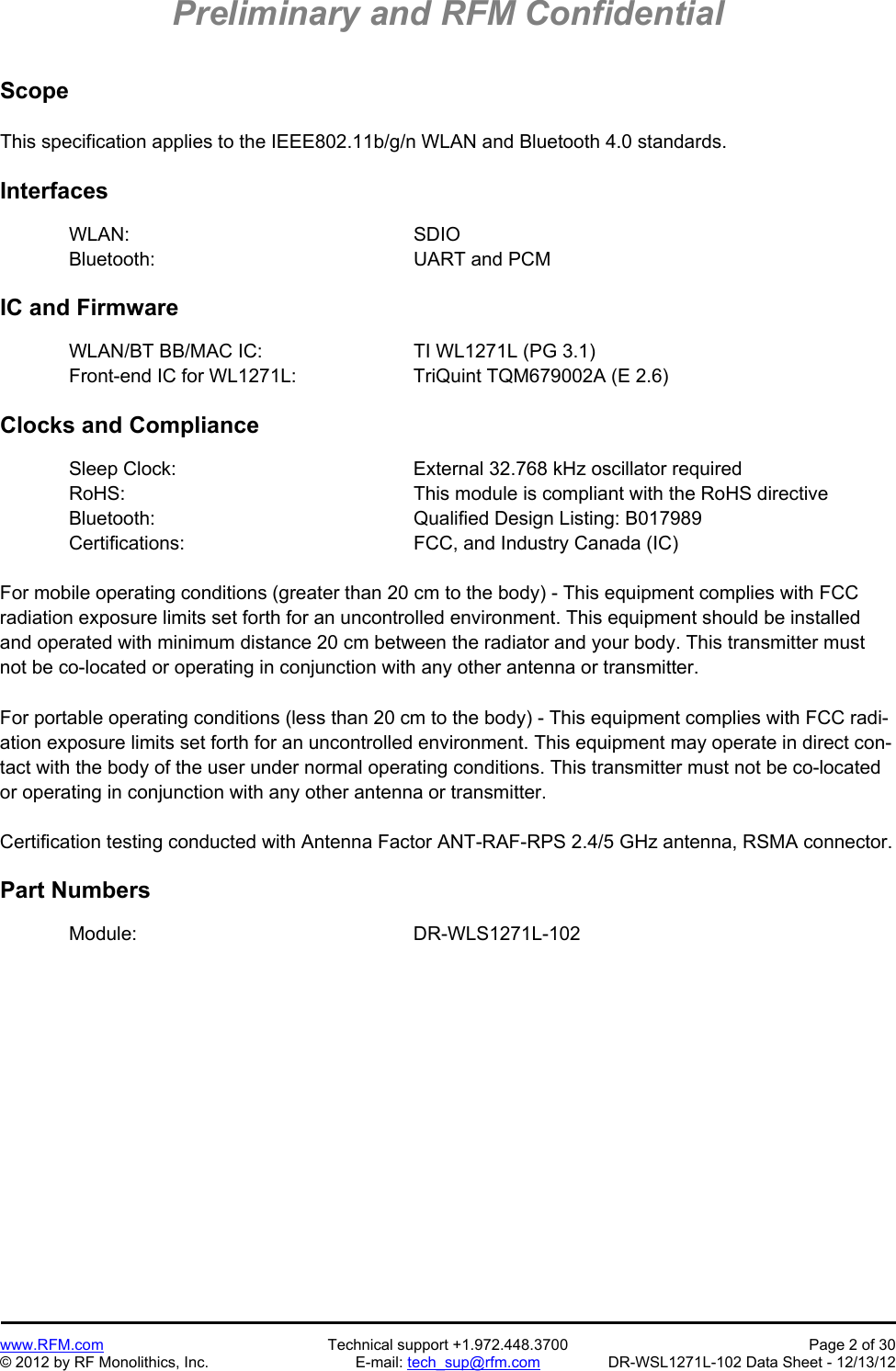
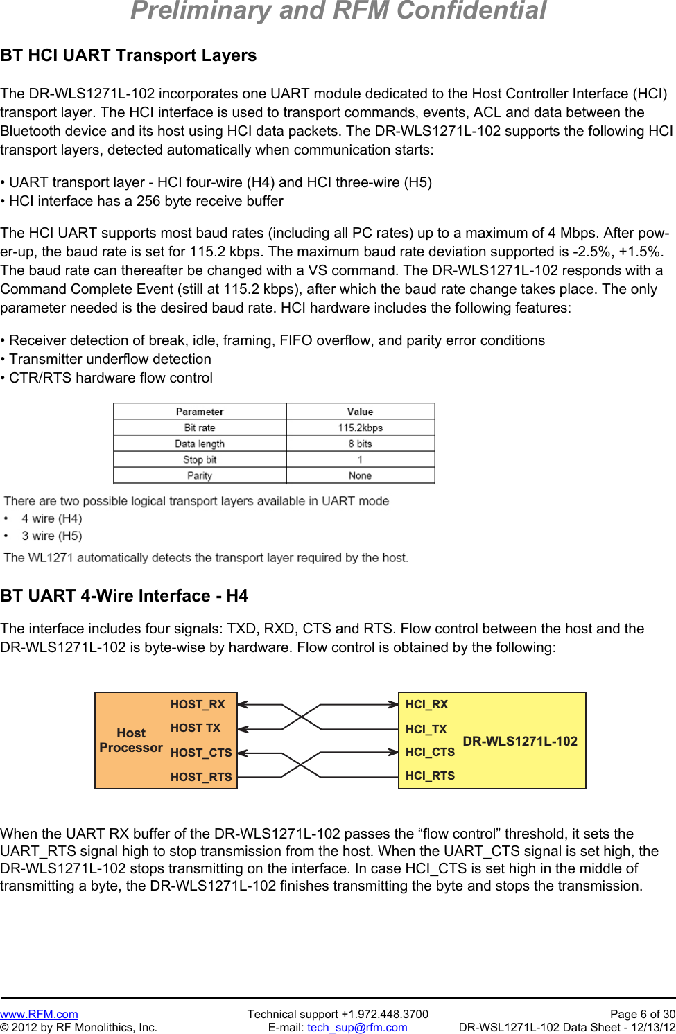
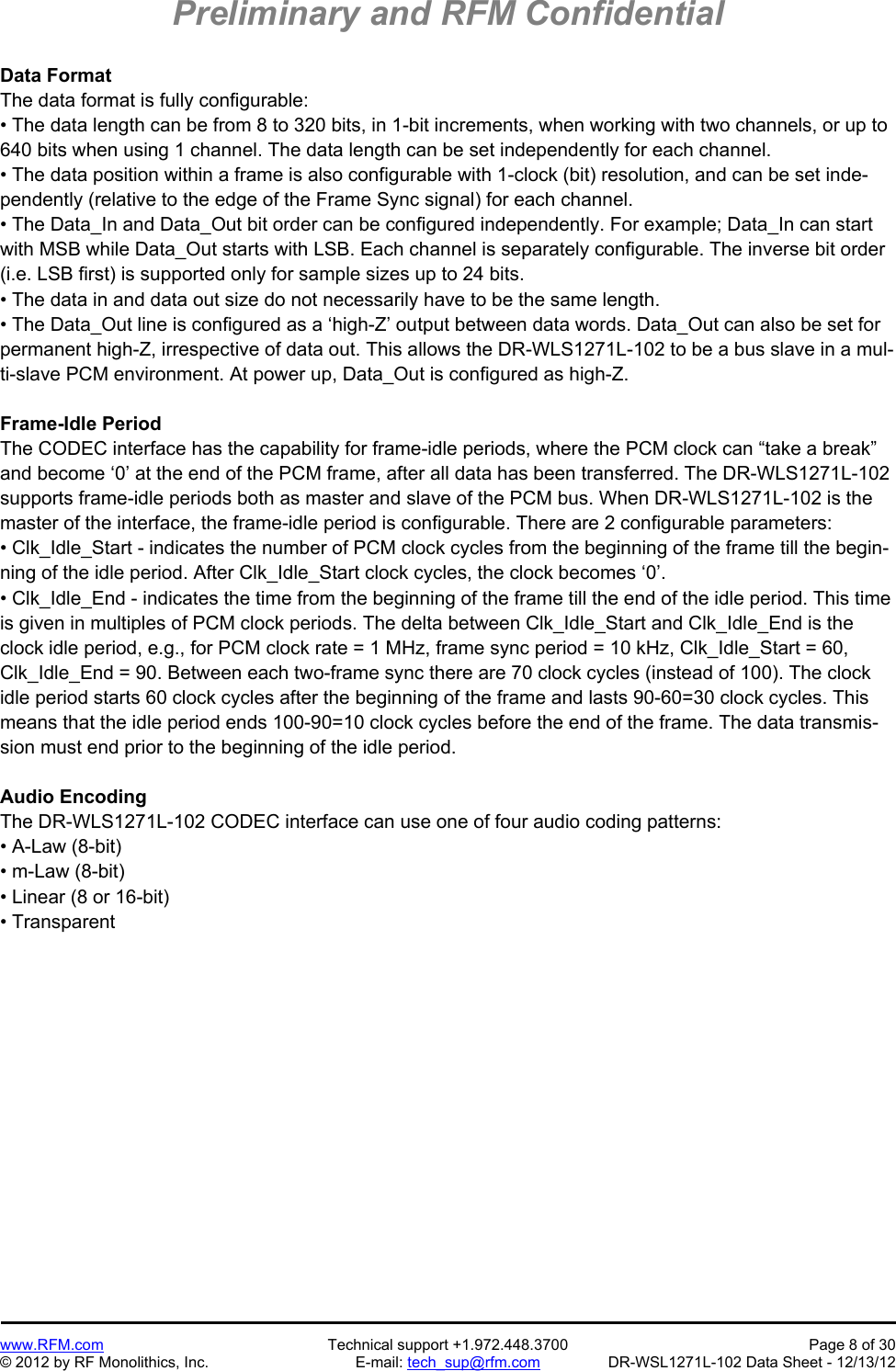
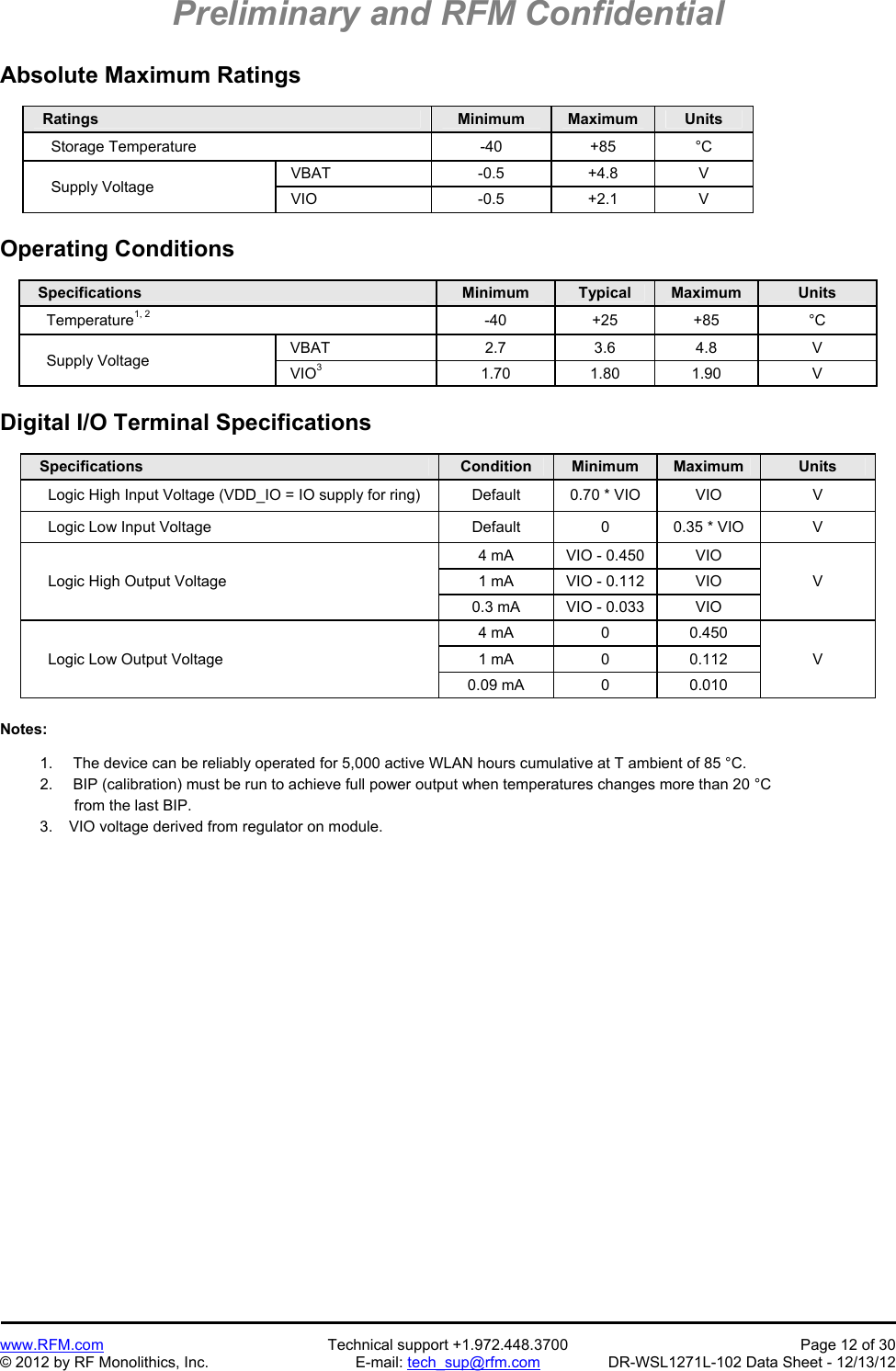
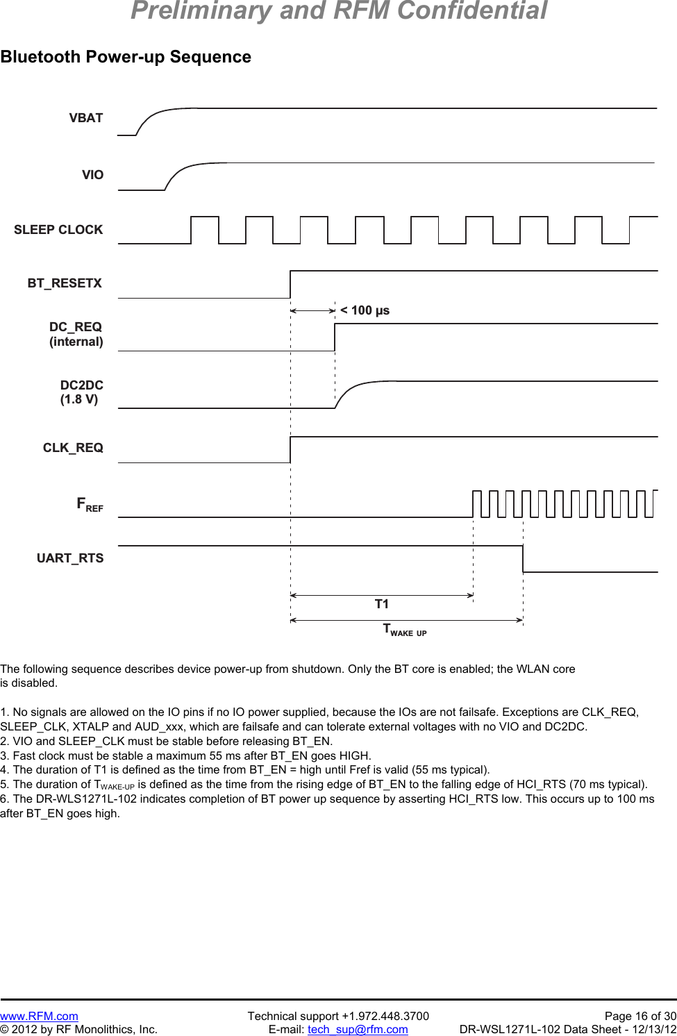
![Preliminary and RFM Confidential www.RFM.com Technical support +1.972.448.3700 Page 3 of 30 © 2012 by RF Monolithics, Inc. E-mail: tech_sup@rfm.com DR-WSL1271L-102 Data Sheet - 12/13/12 Block Diagram 2 . 4 G H zW L A N / B TV I NU A R TP C MS D I OS l o w C L KD C - D CC o n v e r t e r3 8 . 4 M H zF a s t C L KF r o n t E n dI C a n d R FF i l t e r i n gW L 1 2 7 1 LV I OD u a lR e g DR-WLS1271L-102 WLAN Features • WLAN MAC baseband processor and RF transceiver which are IEEE802.11b/g and IEEE802.11n PICS compliant • Optimized for ultra-low current consumption in all operating modes • Accepts 19.2, 26, 38.4, 52 MHz reference clock inputs for easy integration into cellular handsets, etc. • IEEE Standard 802.11d, e, h, i, k, r, PICS compliant • Support for Cisco Client eXtensions (CCX) standard • Serial debug interface • Secure Digital Input/Output (SDIO) host interface • Medium Access Controller (MAC) – Embedded ARM™ central processing unit (CPU) – Hardware-based encryption/decryption using 64-, 128- or 256-bit WEP, TKIP or AES keys – Supports Wi-Fi protected access (WPA and WPA2.0) and IEEE Standard 802.11i, including hardware accelerated Advanced Encryption Standard (AES)] – Designed to work with IEEE Std 802.1x for Virtual Private Network (VPN) solutions • Baseband Processor – IEEE Std 802.11n single-stream data rates (MCS0-7) and SGI support • 2.4 GHz Radio – Digital Radio Processor (DRP) implementation – Integrated LNA – Supports IEEE Std 802.11b, g, b/g and 802.11n](https://usermanual.wiki/Murata-Electronics-North-America/DRWLS1271L/User-Guide-1861480-Page-3.png)