Pycom G01R G01 User Manual
Pycom Ltd G01
UserManual.wiki
>
Pycom
>
G01R User Manual
User Manual
Navigation menu
Upload a User Manual
Namespaces
Wiki Guide
HTML
PDF
Info
Views
User Manual
Discussion / Help
Navigation

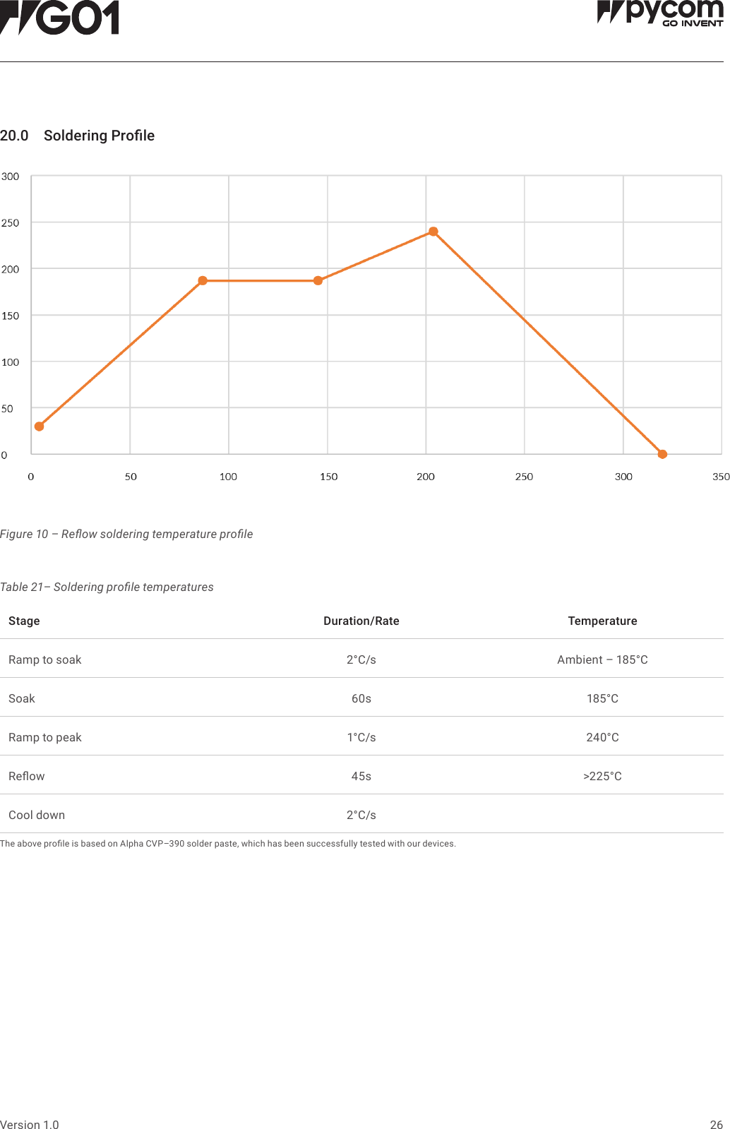
![;7;u-Ѵollmb1-ঞomollbvvbomm|;u=;u;m1;Statement$_bv7;b1;1olrѴb;vb|_-u|ƐƔo=|_;!Ѵ;vĺr;u-ঞombv v0f;1||o|_;=oѴѴobm]|o1om7bঞomvĹ ŐƐő$_bv7;b1;l-mo|1-v;_-ul=Ѵbm|;u=;u;m1;ĺ(2) This device must accept any interference received, including bm|;u=;u;m1;|_-|l-1-v;m7;vbu;7or;u-ঞomĺ &$Ĺ_-m];voulo7bC1-ঞomvmo|;ru;vvѴ-rruo;70|_; party responsible for compliance could void the user's authority to or;u-|;|_;;tbrl;m|ĺNOTE: This equipment has been tested and found to comply with the limits for a Class B digital device, pursuant to Part 15 of |_;!Ѵ;vĺ$_;v;Ѵblb|v-u;7;vb]m;7|oruob7;u;-vom-0Ѵ; ruo|;1ঞom-]-bmv|_-ul=Ѵbm|;u=;u;1;bm-u;vb7;mঞ-Ѵbmv|-ѴѴ-ঞomĺ This equipment generates uses and can radiate radio frequency energy and, if not installed and used in accordance with |_;bmv|u1ঞomvķl-1-v;_-ul=Ѵbm|;u=;u;m1;|ou-7bo 1ollmb1-ঞomvĺo;;uķ|_;u;bvmo]-u-m|;;|_-|bm|;u=;u;m1; bѴѴmo|o11ubm-r-uঞ1Ѵ-ubmv|-ѴѴ-ঞomĺ=|_bv;tbrl;m|7o;v 1-v;_-ul=Ѵbm|;u=;u;m1;|ou-7boou|;Ѵ;bvbomu;1;rঞomķ_b1_ 1-m0;7;|;ulbm;70|umbm]|_;;tbrl;m|o@-m7omķ|_;v;ubv encouraged to try to correct the interference by one or more of the following measur es:Ŋ!;oub;m|ouu;Ѵo1-|;|_;u ;1;bbm]-m|;mm-ĺ Ŋm1u;-v;|_;v;r-u-ঞom0;|;;m|_;;tbrl;m|-m7u;1;b;uĺ Ŋomm;1||_;;tbrl;m|bm|o-mo|Ѵ;|om-1bu1b|7b@;u;m|=uol |_-||o_b1_|_;u;1;b;ubv1omm;1|;7ĺŊomvѴ||_;7;-Ѵ;uou-m;r;ub;m1;7u-7boņ$(|;1_mb1b-m=ou_;ѴrĺRF Warning StatementThis device is intended only for OEM integrators m7;u|_;=oѴѴobm]1om7bঞomvĹ1) The antenna must be installed such that 20 cm is maintainedbetween the antenna and users, andƑő $_;|u-mvlb;ulo7Ѵ;l-mo|0;1oŊѴo1-|;7b|_-mo|_;u|u-mvlb;uou-m|;mm-ĺvѴom]-v|o1om7bঞomv-0o;-u;l;|ķ=u|_;u|u-mvlb;u|;v|bѴѴmo|0;u;tbu;7ĺo;;uķ|_;bm|;]u-|oubvvঞѴѴu;vromvb0Ѵ;=ou|;vঞm]|_;bu;m7Ŋruo71|=ou-m-77bঞom-Ѵ1olrѴb-m1;u;tbu;l;m|vu;tbu;7b|_|_bvlo7Ѵ;bmv|-ѴѴ;7ĺ$o;mvu;1olrѴb-m1;b|_-ѴѴmomŊ|u-mvlb;u=m1ঞomv|_;_ov|manufacturer is responsible for ensuring compliance with the lo7Ѵ;Ővőbmv|-ѴѴ;7-m7=ѴѴor;u-ঞom-Ѵĺou;-lrѴ;ķb=-_ov|-vru;bovѴ-|_oub;7-v-mmbm|;mঞom-Ѵu-7b-|oum7;u|_;;1Ѵ-u-ঞomo=om=oulb|ruo1;7u;b|_o|-|u-mvlb;u1;uঞC;7module and a module is added, the host manufacturer is responsible =ou;mvubm]|_-||_;-[;u|_;lo7Ѵ;bvbmv|-ѴѴ;7-m7or;u-ঞom-Ѵ|_;_ov|1omঞm;v|o0;1olrѴb-m|b|_|_;-u|ƐƔmbm|;mঞom-Ѵu-7b-|ouu;tbu;l;m|vĺ$_;lo7Ѵ;bvѴblb|;7|obmv|-ѴѴ-ঞom+ĺ$_;lo7Ѵ;bvѴblb|;7|obmv|-ѴѴ-ঞombmlo0bѴ;ouC;7-rrѴb1-ঞomĺWe hereby acknowledge our responsibility to provide guidance to the host manufacturer in the event that they require assistance for ;mvubm]1olrѴb-m1;b|_|_;-u|ƐƔ"0r-u|u;tbu;l;m|vĺ!$$$Ĺm|_;;;m||_-||_;v;1om7bঞomv1-mmo|0;l;|Ő=ou;-lrѴ;1;u|-bmѴ-r|or1omC]u-ঞomvou1oŊѴo1-ঞomb|_-mo|_;u|u-mvlb;uőķ|_;m|_;-|_oub-ঞombvmolonger considered valid and the FCC ID cannot be used on the Cm-Ѵruo71|ĺm|_;v;1bu1lv|-m1;vķ|_;bm|;]u-|oubѴѴ0;u;vromvb0Ѵ;=ouu;;-Ѵ-ঞm]|_;;m7ruo71|Őbm1Ѵ7bm]|_;|u-mvlb;uő-m7o0|-bmbm]-v;r-u-|;-|_oub-ঞomĺEnd Product Labeling-m-Ѵm=oul-ঞom|o|_;m7&v;u$_;bm|;]u-|ou_-v|o0;--u;mo||oruob7;bm=oul-ঞom|o|_;;m7v;uu;]-u7bm]_o|obmv|-ѴѴouu;lo;|_bv!lo7Ѵ;bm|_;v;uĽvl-m-Ѵo=|_;;m7ruo71|_b1_bm|;]u-|;v|_bvlo7Ѵ;ĺIn the user manual of the end product, the end user has to be informed that the equipment complies with FCC radio-frequency ;rovu;]b7;Ѵbm;vv;|=ou|_=ou-mm1om|uoѴѴ;7;mbuoml;m|ĺThe end user has to also be informed that any changes or lo7bC1-ঞomvmo|;ru;vvѴ-rruo;70|_;l-m=-1|u;u1oѴ7ob7|_;v;uŝv-|_oub||oor;u-|;|_bv;tbrl;m|ĺThe end user manual shall include all required regulatory bm=oul-ঞomņ-umbm]-vv_obm|_bvl-m-ѴĺThis equipment complies with FCC radiation exposure limits set forth for an uncontrolled environment .This equipment should be installed and operated withminimum distance 20cm between the radiator& your body.The outside of final products that contains this module device must display a label referring to theenclosedmodule. This exterior label can use wording such as: "Contains Transmitter Module FCC ID:2AJMTG01R,&*5 or “Contains FCC ID:2AJMTG01R,&*5 , Any similar wording that expresses the same meaning may be used.6LQJOH0RGXODU$SSURYDO2XWSXWSRZHULVFRQGXFWHG7KLVGHYLFHLVWREHXVHGLQPRELOHRUIL[HGDSSOLFDWLRQVRQO\$QWHQQDJDLQLQFOXGLQJFDEOHORVVPXVWQRWH[FHHG G%LIRUWKHSXUSRVHRIVDWLVI\LQJWKHUHTXLUHPHQWVRI&)57KHDQWHQQDVXVHGIRUWKLVWUDQVPLWWHUPXVWEHLQVWDOOHGWRSURYLGHDVHSDUDWLRQGLVWDQFHRIDWOHDVWFPIURPDOOSHUVRQVDQGPXVWQRWEHFRORFDWHGRURSHUDWHGLQFRQMXQFWLRQZLWKDQ\DQWHQQDRUWUDQVPLWWHUH[FHSWLQDFFRUGDQFHZLWK)&&PXOWLWUDQVPLWWHUHYDOXDWLRQSURFHGXUH&RPSOLDQFHRIWKLVGHYLFHLQDOOILQDOSURGXFWFRQILJXUDWLRQVLVWKHUHVSRQVLELOLW\RIWKH*UDQWHH,QVWDOODWLRQRIWKLVGHYLFHLQWRVSHFLILFILQDOSURGXFWVPD\UHTXLUHWKHVXEPLVVLRQRID&ODVV,,SHUPLVVLYHFKDQJHDSSOLFDWLRQFRQWDLQLQJGDWDSHUWLQHQWWR5)([SRVXUHVSXULRXVHPLVVLRQV(53(,53DQGKRVWPRGXOHDXWKHQWLFDWLRQRUQHZDSSOLFDWLRQLIDSSURSULDWH7 @ FDD (Band 4),10.51 @ FDD (Band 12) and 10.94 @ FDD (Band 13)ISED RSS Warning/ISED RF Exposure Statement/HSUpVHQWDSSDUHLOHVWFRQIRUPHDX[&15G,6('DSSOLFDEOHVDX[DSSDUHLOVUDGLRH[HPSWVGHOLFHQFH/H[SORLWDWLRQHVWDXWRULVpHDX[GHX[FRQGLWLRQVVXLYDQWHVODSSDUHLOQHGRLWSDVSURGXLUHGHEURXLOODJHHWOXWLOLVDWHXUGHODSSDUHLOGRLWDFFHSWHUWRXWEURXLOODJHUDGLRpOHFWULTXHVXELPrPHVLOHEURXLOODJHHVWVXVFHSWLEOHGHQFRPSURPHWWUHOHIRQFWLRQQHPHQW,6('5)H[SRVXUHVWDWHPHQW/HUD\RQQHPHQWGHODFODVVHEUHSHFWH,6('IL[DLHQWXQHQYLURQQHPHQWQRQFRQWU{OpV,QVWDOODWLRQHWPLVHHQ°XYUHGHFHPDWpULHOGHYUDLWDYHFpFKDQJHXUGLVWDQFHPLQLPDOHHQWUHFPWRQFRUSV/DQFHXUVRXQHSHXYHQWSDVFRH[LVWHUFHWWHDQWHQQHRXFDSWHXUVDYHFG¶DXWUHVThe product only use ceramic antenna for Bluetooth and wifi which the antenna gain is 1.3 dBi integration in a hostFor IC , to meet RF exposure & ERP/ERIP, the maximum net gain of antennas allowed are 5.96 dBi @ FDD (Band 4), 7.14 @ FDD (Band 12) and 7.46 @ FDD (Band 13). The antenna(s) used for this transmitter must be installed to provide a separation distance of at least 20 cm from all persons and must not be co-located or operating in conjunction with any other antenna or transmitter.](https://usermanual.wiki/Pycom/G01R/User-Guide-3889103-Page-29.png)