RELM Communications RPU416A UHF FM Transceiver User Manual Service Manual
RELM Communications Inc UHF FM Transceiver Service Manual
UserManual.wiki
>
RELM Communications
>
RPU416A User Manual
>
Service Manual
Contents
1.
Users Manual
2.
Service Manual
3.
New Alignment Manual
4.
Revised Manual
Service Manual
Navigation menu
Upload a User Manual
Namespaces
Wiki Guide
HTML
PDF
Info
Views
User Manual
Discussion / Help
Navigation
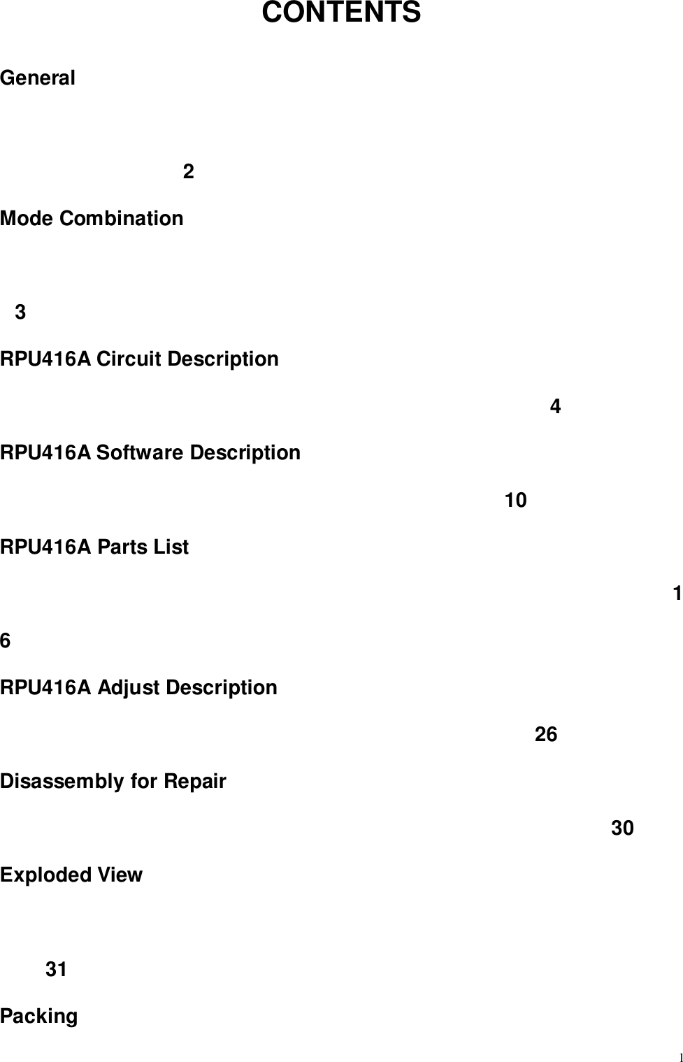

![9RPU416A Circuit Descriptionswitching circuit before it is passed to the antenna terminal. The transmit/receive switching circuit iscomprised of D101, D102 and D103. D102 and D103 turned on (conductive ) in transmit mode and off(isolated) in receive mode.5) APCThe automatic power control (APC) circuit stabilizes the transmitter output power at a predeterminedlevel by sensing the drain current of the final amplifier Field Effect Transistor (FET). The voltage obtainedfrom the above drain current with a reference voltage which is set using the microprocessor. An APCvoltage proportional to the difference between the sensed voltage and the reference voltage appears atthe output of IC100 (1/2). This output voltage controls the gate of the FET power amplifier, which keepsthe transmitter output power can be varied by the microprocessor which in turn changes the referencevoltage and hence , the output power.6) Terminal protection circuitWhen the thermistor (TH102) reaches about 80", the protection circuit turns on Q110 to protecttransmitting final amplifier (Q107).5. Power supplyA 5V reference power supply [5M] for the control circuit is derived from an internal battery. Thisreference is used to provide a 5V supply in transmit mode [5T] ,a 5V supply in receive mode [5R] , and a5V, supply common in both modes [5C] based on the control signal sentfrom the microprocessor.6. Control systemThe IC403 CPU operates at 7.37MHZ. This oscillator has a circuit that shifts the frequency according tothe EEPROM data.](https://usermanual.wiki/RELM-Communications/RPU416A.Service-Manual/User-Guide-233592-Page-9.png)
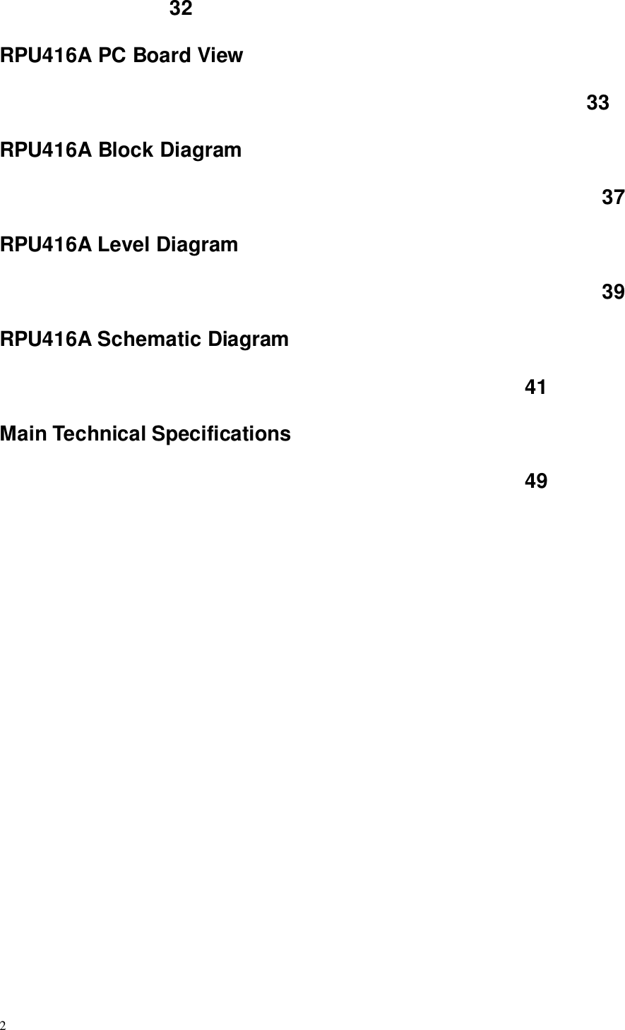
![11(3) Press [MONI],then press [PTT], to set the channel, channel data and initial data.(4) Turn off the power, disconnect SELF on PCB to end mode settings.(5) Remarks:The old data(frequency, CTCSS/DQT, channel function) will be deleted once set the newmode by pressing MONI AND PTT , part of the function also would be changed. Therefore, donot set this operation unless change the EEPROM, etc.](https://usermanual.wiki/RELM-Communications/RPU416A.Service-Manual/User-Guide-233592-Page-11.png)
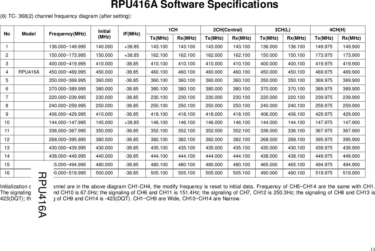
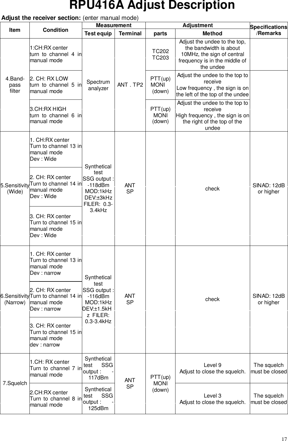
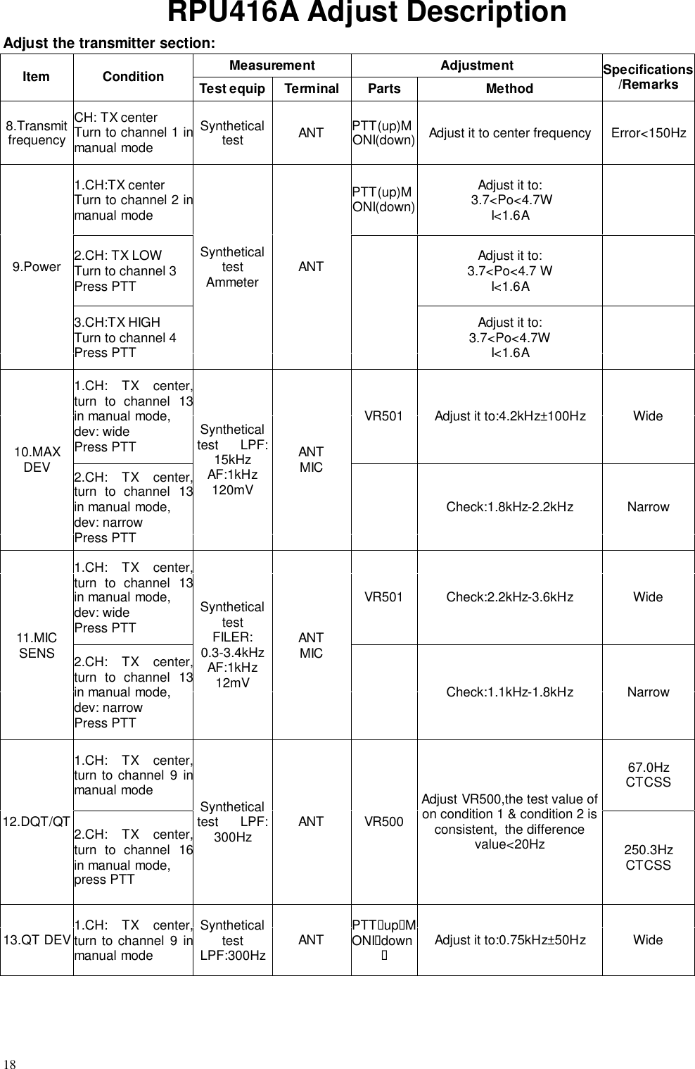
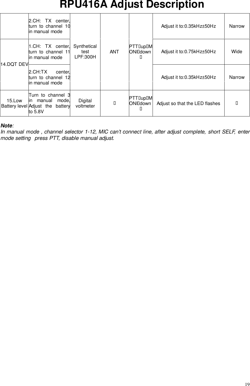
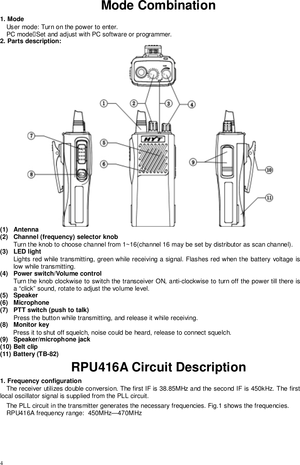
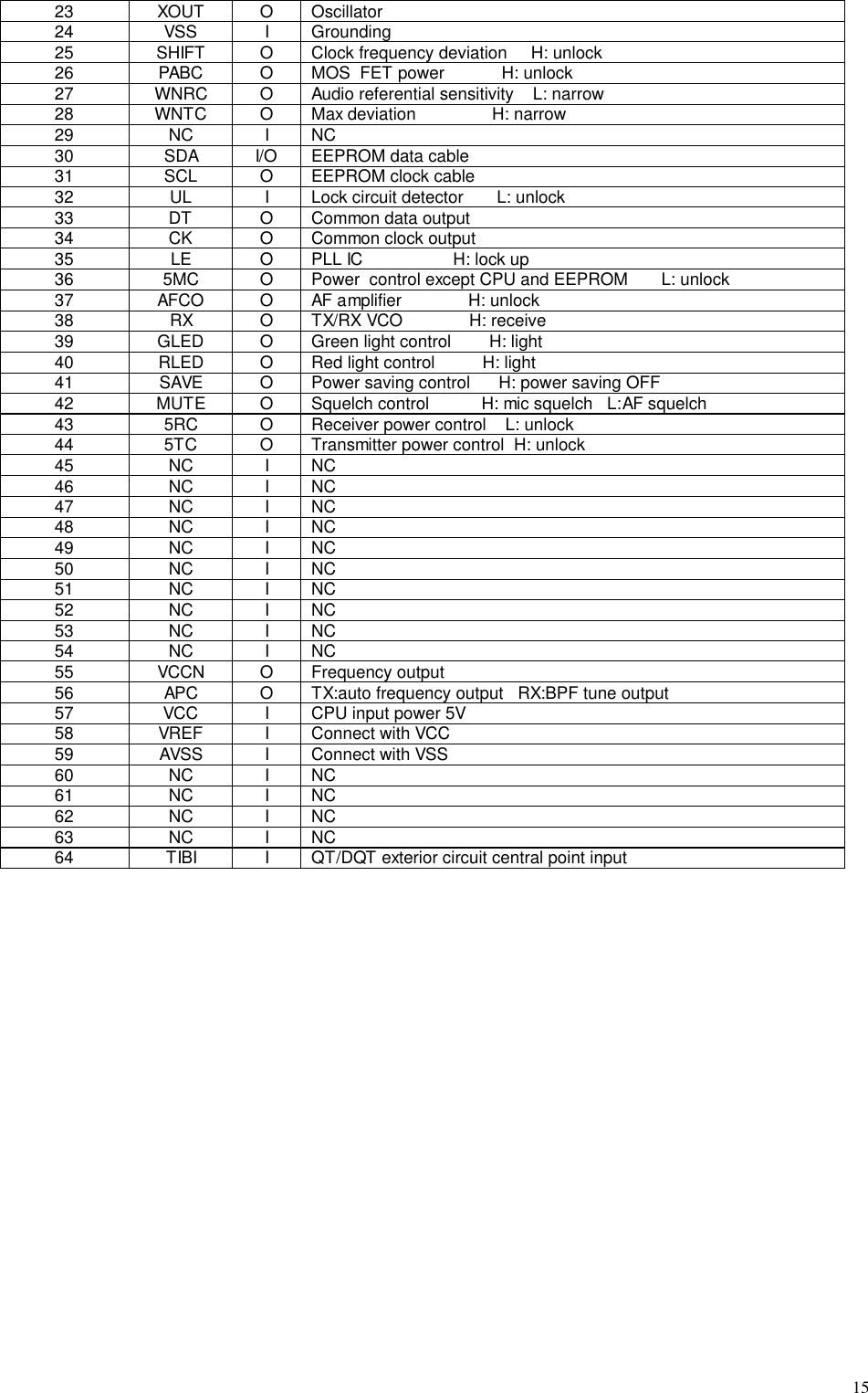
![14RPU416A Software Specifications6. Manual Adjust Mode:Press PTT and MONI simultaneously to turn on the power"enter manual Adjust mode out 3seconds later. Choose the settings by turning the channel selector knob 1-12CH, use PTT(upward) or MONI (downward) to adjust (Notice: MIC shouldn’t be connected with external cablewhile modifying),1~12CH are defined as follows:(1) Frequency stability(2) RF power(3) Low power alarm(4) Receiver sensitivity (center frequency adjust)(5) Receiver sensitivity (low frequency adjust)(6) Receiver sensitivity (high frequency adjust)(7) Squelch (level 9)(8) Squelch (level 3)(9) CTCSS deviation (Wide)(10) CTCSS deviation (Narrow)(11) DQT deviation (Wide)(12) DQT deviation (Narrow)13~16CH are used for adjusting transmitter and receiver. Press PTT to transmit; Press MONIto choose: Wide/Narrow, one Beep sound is Narrow, two Beep sound is Wide. 13~16CH aredefined as follows:(13) center frequency (discrepancy of transmission and receive frequency is 0.1MHz).(14) Lowest frequency (discrepancy of transmission and receive frequency is 0.1MHz).(15) Highest frequency (discrepancy of transmission and receive frequency is -0.075MHz).(16) center frequency: sends 250.3Hz CTCSS signals (discrepancy of transmission and receivefrequency is 0.1MHz).Note:To enter and shut off manual adjust mode by short cut the SELF. Turn on the power, and entersettings mode, the manual function is automatically on. Press [PTT] to disable manual modify. Oncethis function is disabled, this mode is not accessible, kindly suggest disable this mode after adjust.. CPU:CPU control M38034M4Pin No. Portname I/O Function1 TI I Input QT/DQT signal2 BUSY I Input busy signal3 BATT I Detect battery voltage4NCINC5 TO O Output QT/DQT6 BEEP O Beep output7NCINC8 ENC0 I Input encode9 ENC1 I Input encode10 ENC2 I Input encode11 ENC3 I Input encode12 NC I NC13 PTT I [PTT] input ,connect RXD14 TXD O RS-232C outputRPU416A Software Specifications15 RXD I RS-232C inputx16 MONI I [MONI] input17 SELF I Program L: set up mode18 CNVSS I Connect VSS19 RST I Reset20 INT0 I Power detection21 NC I NC22 XIN I Oscillator(7.3728MHz)](https://usermanual.wiki/RELM-Communications/RPU416A.Service-Manual/User-Guide-233592-Page-14.png)
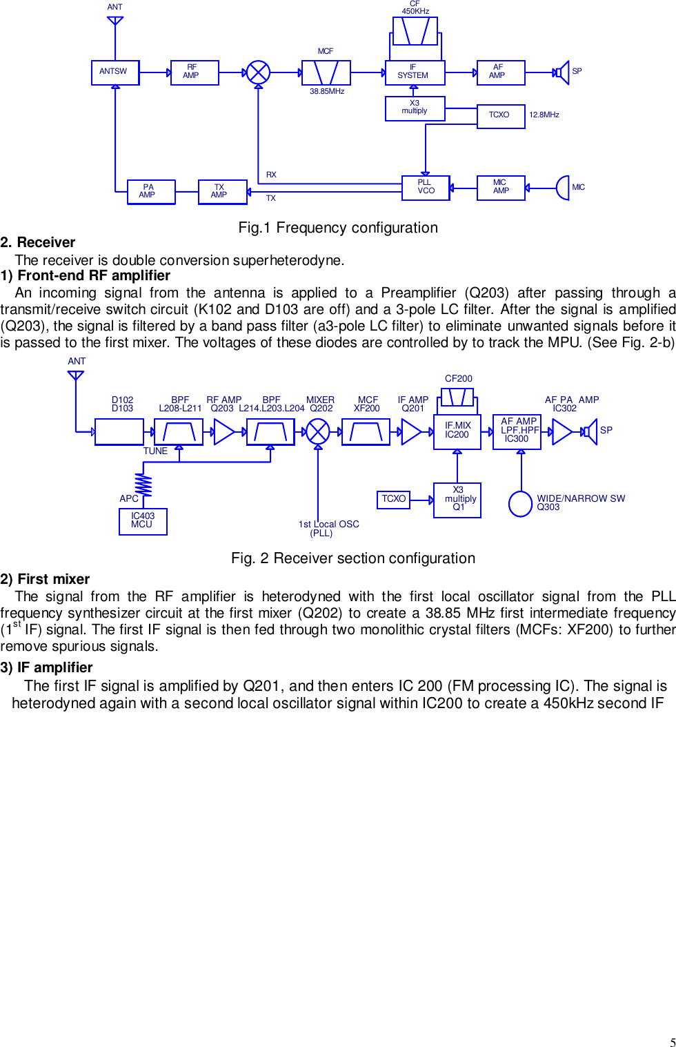
![16RPU416A Adjust DescriptionUse programmer or PC software to program RPU416A, or by manual program, refer to”RPU416Asoftware description ” for the manual program and mode settings.. Instrument:1. Synthesized test instrument 1 set2. Scanner 1 set3. 3A/10V power 1 set4. Digital Voltmeter 1 set5. 3A DC Ammeter 1 set. Adjust:1. Initialization"It is necessary to initialize the transceiver because there is useless data in EEPROM. Short cut theSELF on PCB, turn on the power till there comes the sound ”BEEP”, place the channel selectorknob, press [MONI], then press [PTT], to begin initializing the channel and other data. Please referto the outcome of initialization at”RPU416A software description”.2.Adjustment:The adjustment of RPU416A, some are conducted in normal mode, some are in manual programmode. Turn on the power and enter the normal mode., at the same time, press the PTT and MONIto turn on the transceiver"enter the manual program mode 3seconds later.(refer to”RPU416Asoftware description” manual program mode).VCO SECTION:measurement AdjustmentITEM CONDITION Test equip terminal part MethodSpecifications/Remarks1.Setting 1.power 7.5V1.CH: TX HIGH 3.7V±0.1V2.TransmitVCO lockvoltage 2.CH: TX LOW check RPU416A >1V1.CH: RX HIGH 3.7V±0.1V3.ReceiveVCO lockvoltage 2.CH: RX LOWDigitalVolt meter CV TC1check RPU416A>1VNote:If unlock VCO, check adjustment is enabled in manual mode.(signal could be transmitted regardless of thelock of VCO in manual mode).](https://usermanual.wiki/RELM-Communications/RPU416A.Service-Manual/User-Guide-233592-Page-16.png)