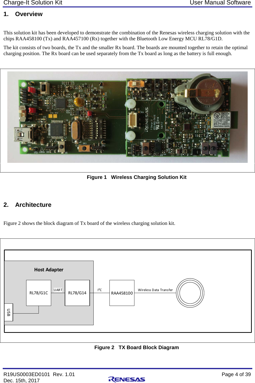
Renesas Electronics Europe CHARGE-IT Evaluation Board User Manual
Renesas Electronics Europe GmbH Evaluation Board Users Manual
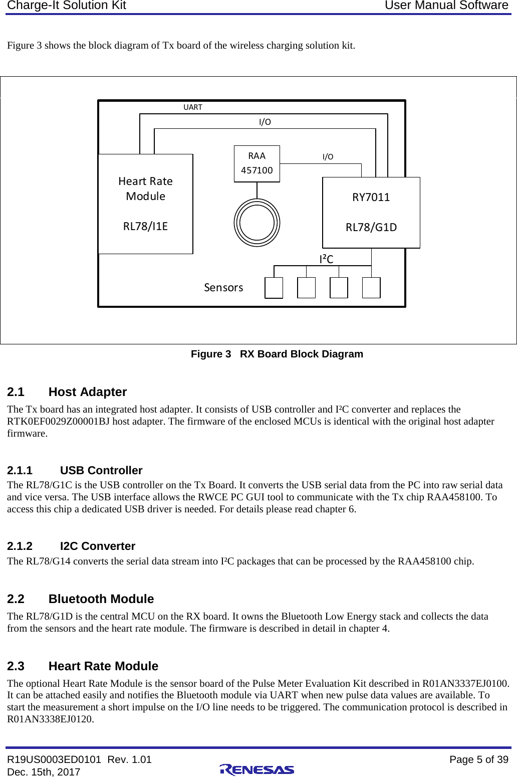
UserManual.wiki
>
Renesas Electronics Europe
>
CHARGE IT User Manual
Users Manual
Navigation menu
Upload a User Manual
Namespaces
Wiki Guide
HTML
PDF
Info
Views
User Manual
Discussion / Help
Navigation
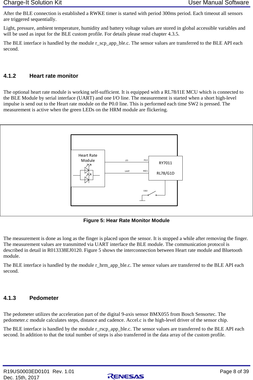
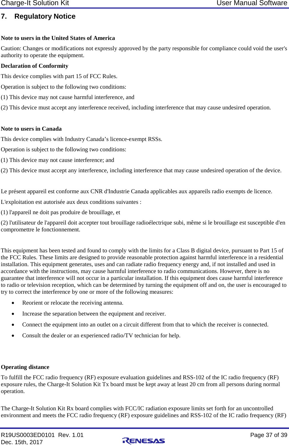
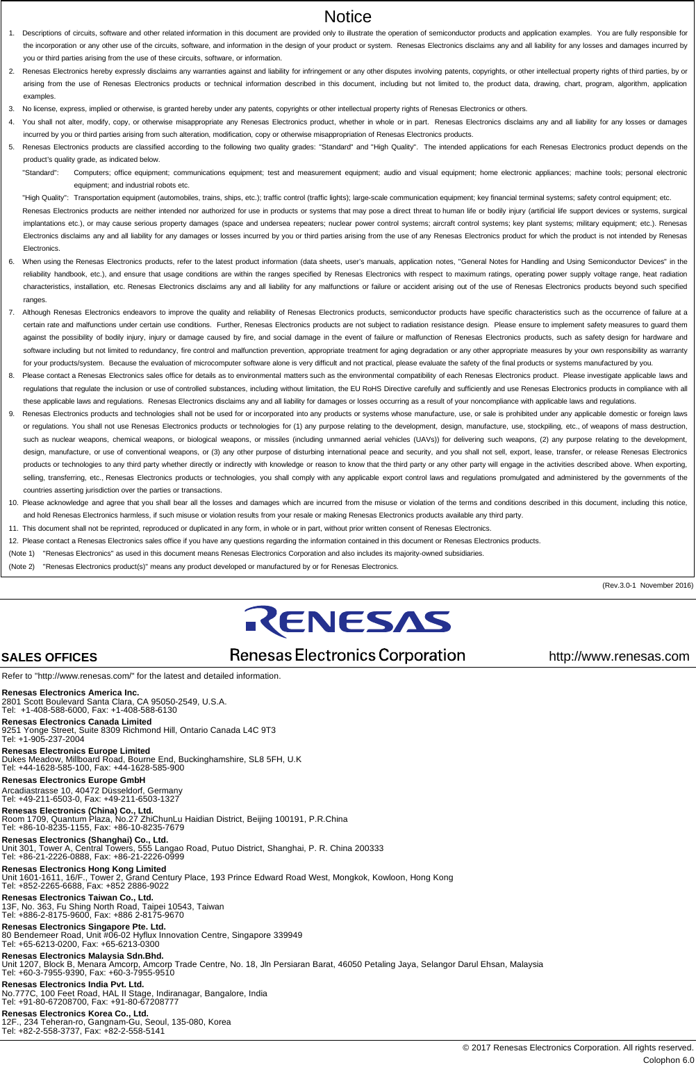
![Charge-It Solution Kit User Manual Software R19US0003ED0101 Rev. 1.01 Page 17 of 39 Dec. 15th, 2017 4.4 Advertising Table 6 shows the settings of advertising. Table 6: Advertising specification Advertising Type Connectable undirected advertising (ADV_IND) Advertising Interval Min Default: 20 [ms] Advertising Interval Max Default: 60 [ms] Advertising Channel Map All Channels (37, 38, 39 ch) Advertising Data - Length of this Data 2 [bytes] Data Type <<Flags>> (0x01) Flags LE General Discoverable Mode BR/EDR Not Supported Length of this Data 9 [bytes] Data Type <<Complete Local Name>> (0x09) Local Name CHARGE-IT Length of this Data 3 [bytes] Data Type << Complete List of 16-bit Service Class UUIDs>> (0x03) UUID 0x180A (Device Information Service) Length of this Data 3 [bytes] Data Type << Complete List of 16-bit Service Class UUIDs>> (0x03) UUID 0x180D (Heart Rate Service) Length of this Data 3 [bytes] Data Type << Complete List of 16-bit Service Class UUIDs>> (0x03) UUID 0x1814 (Running Speed & Cadence Service) Length of this Data 3 [bytes] Data Type << Complete List of 16-bit Service Class UUIDs>> (0x03) UUID 0x1809 (Heath Thermometer Service) Scan Response Data none](https://usermanual.wiki/Renesas-Electronics-Europe/CHARGE-IT/User-Guide-3753059-Page-17.png)
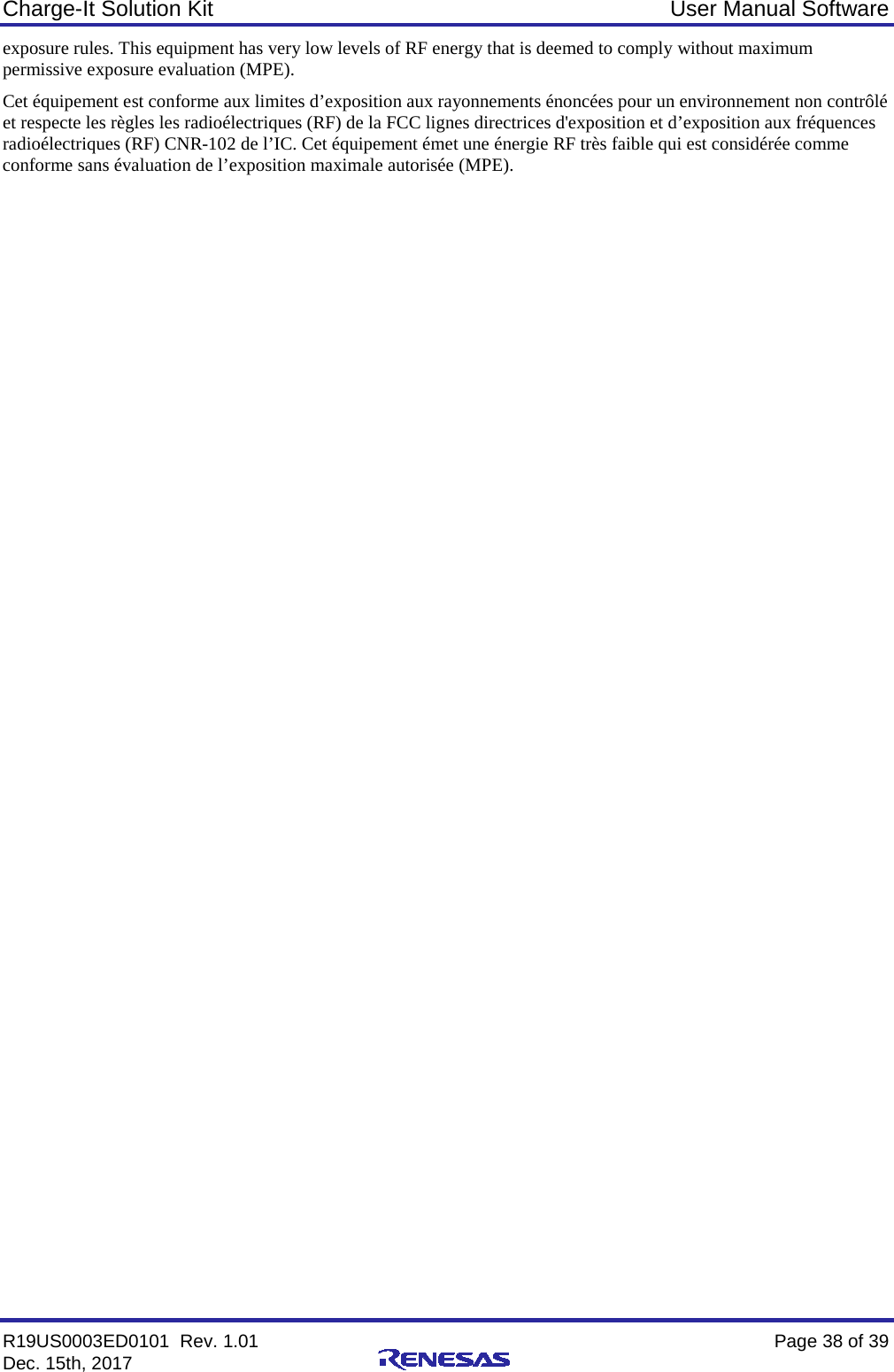
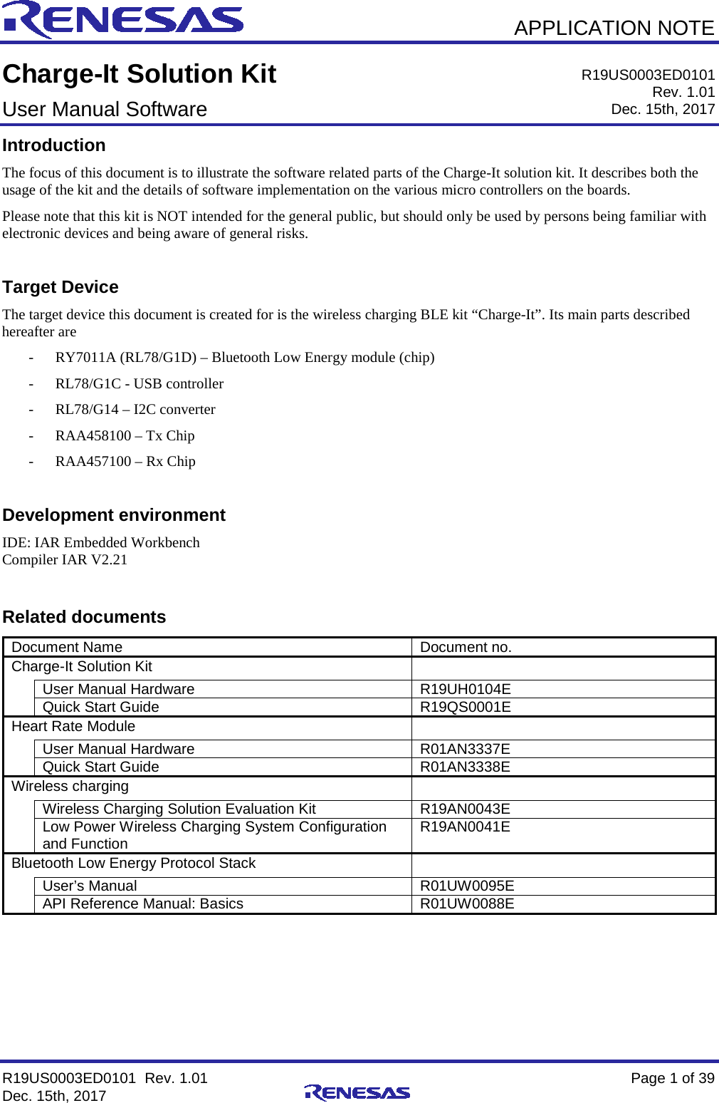
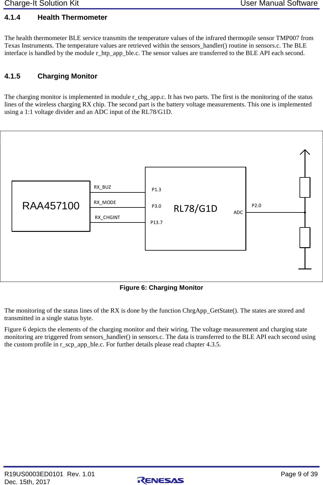
![Charge-It Solution Kit User Manual Software R19US0003ED0101 Rev. 1.01 Page 18 of 39 Dec. 15th, 2017 4.5 Connection Table 7 shows the settings of connection. Table 7: Connection specification Scan Interval 30 [ms] Scan Window Size 30 [ms] Initiator Filter Policy Ignore White List Own Address Type Public Address Minimum of Connection Interval 30 [ms] Maximum of Connection Interval 50 [ms] Connection Latency 0 [ms] Link Supervision Timeout 5 [s] Minimum CE Length 0 [ms] Maximum CE Length 50 [ms] 4.6 Pairing Table 8 shows the settings of pairing. Table 8: Pairing specification Bonding Bondable Mode Security Mode Unauthenticated pairing with encryption Pairing Method Just Works IO capability No Input No Output OOB flag OOB Data not present Authentication Requirements No MITM Bonding Encryption key size 128 [bit] Initiator key distribution None Responder key distribution Encryption key](https://usermanual.wiki/Renesas-Electronics-Europe/CHARGE-IT/User-Guide-3753059-Page-18.png)
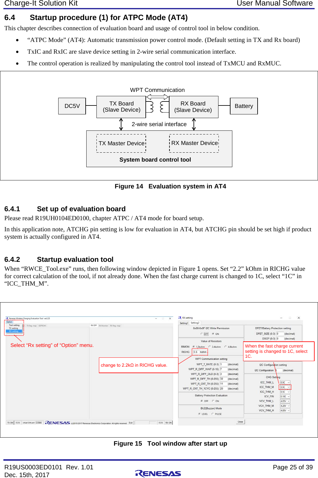
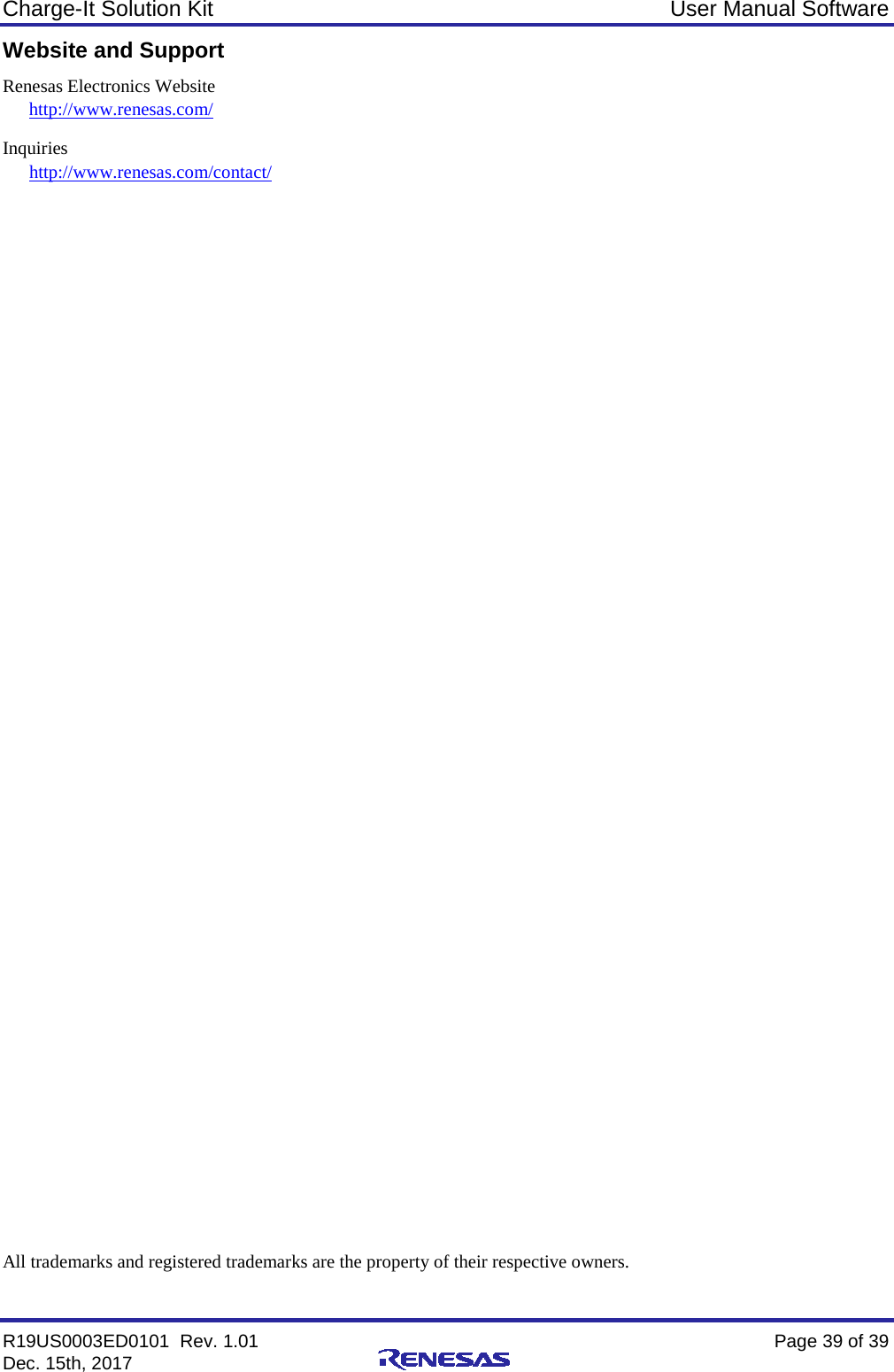
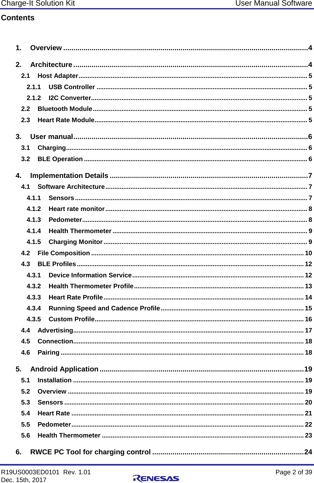
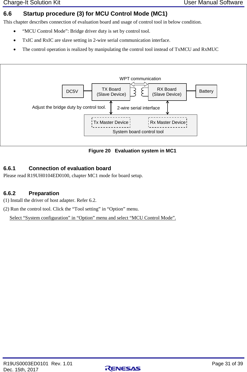
![Charge-It Solution Kit User Manual Software R19US0003ED0101 Rev. 1.01 Page 28 of 39 Dec. 15th, 2017 6.5 Startup procedure (2) for ATPC Mode (AT1) This chapter describes connection of evaluation board and usage of control tool in below condition. • “ATPC Mode” (AT1). Automatic transmission power control mode. • TxIC and RxIC are master setting in 2-wire serial communication interface. • Register setting is read from the EEPROM in TX board. Figure 17 Evaluation system in AT1 6.5.1 Writing method to EEPROM in TX board The control tool has EEPROM Write/Read tool. This section describes the procedure that necessary data is written into EEPROM in below condition. • PWM initial duty is 20[%], fast charge current is 0.5xICHGR. 6.5.2 Set up of evaluation board Please read R19UH0104ED0100, chapter ATPC / AT4 mode for board setup. 6.5.3 Startup procedure of EEPROM Write/Read tool (1) Turn on SW14 of TX board, Supply DC5V to TX board. (2) When “RWCE_Tool.exe” run, then following window opens. (3) When “TX setting” in “Option” menu is selected, TX setting window opens. (4) Select ”Master” in Setting1 window, then click “Close” button TX Board (Master Device) RX Board (Master Device) TX ROM (Slave Device) DC5V Battery 2-wire serial interface WPT communication](https://usermanual.wiki/Renesas-Electronics-Europe/CHARGE-IT/User-Guide-3753059-Page-28.png)
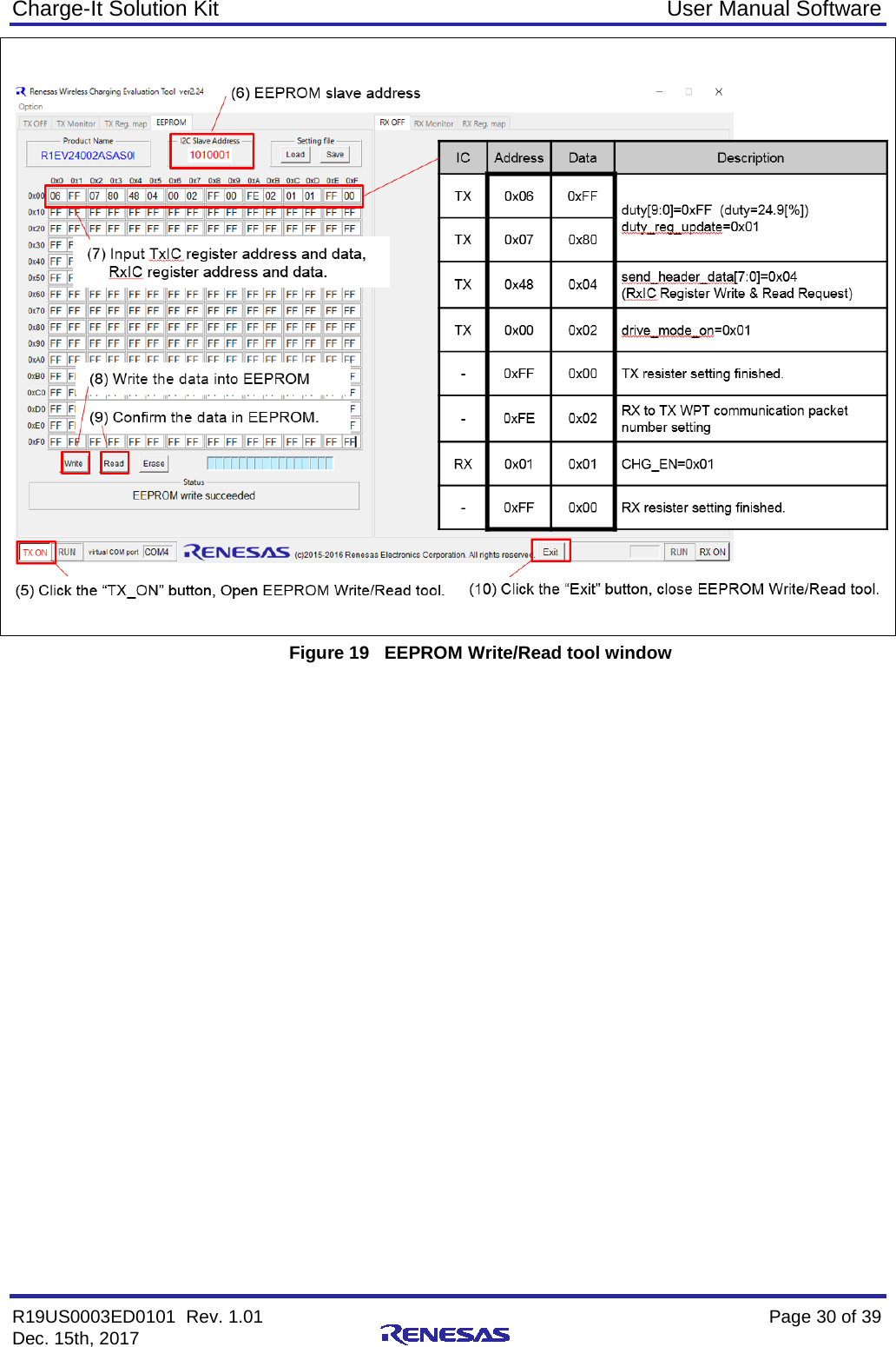
![Charge-It Solution Kit User Manual Software R19US0003ED0101 Rev. 1.01 Page 29 of 39 Dec. 15th, 2017 Figure 18 2-wire serial communication interface Slave/Master setting of TxIC in control tool (5) When “TX ON” button is pushed, EEPROM Write / Read control tool opens. (Figure 19) (6) Input EEPROM slave address into “I2C Slave Address”. Because default value is ”1010001” and EEPROM address setting of TX board is ”1010001”, Input address is not necessary. (7) Input TX register address and data, RX register address and data into EEPROM tool window. For example, Figure 4.4 shows register setting that bridge duty is 25 [%] and fast charge current is 0.5xICHGR. Because the condition that fast charge current is 0.5xICHGR is default setting, RxIC register setting is only that CHG_EN is ON. (8) When the “Write” button in tool window is clicked, data is written into EEPROM. (9) When the “Read” button in tool window is clicked, written data in EEPROM is displayed. Confirm the EEPROM data. (10) Click the “Exit” button in tool window, then close the control tool. (11) Remove host adaptor output cable from TX board, Turn off the SW14 of TX board. (3) Select ”TX Setting” in “Option” menu. (4) Select “Master” in “Setting1”,then click “Close” bottom.](https://usermanual.wiki/Renesas-Electronics-Europe/CHARGE-IT/User-Guide-3753059-Page-29.png)
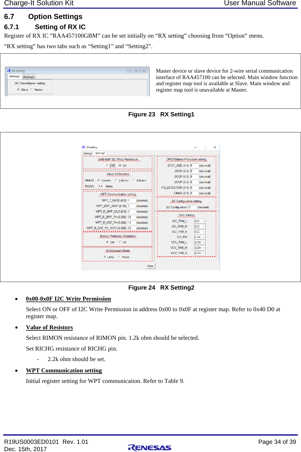
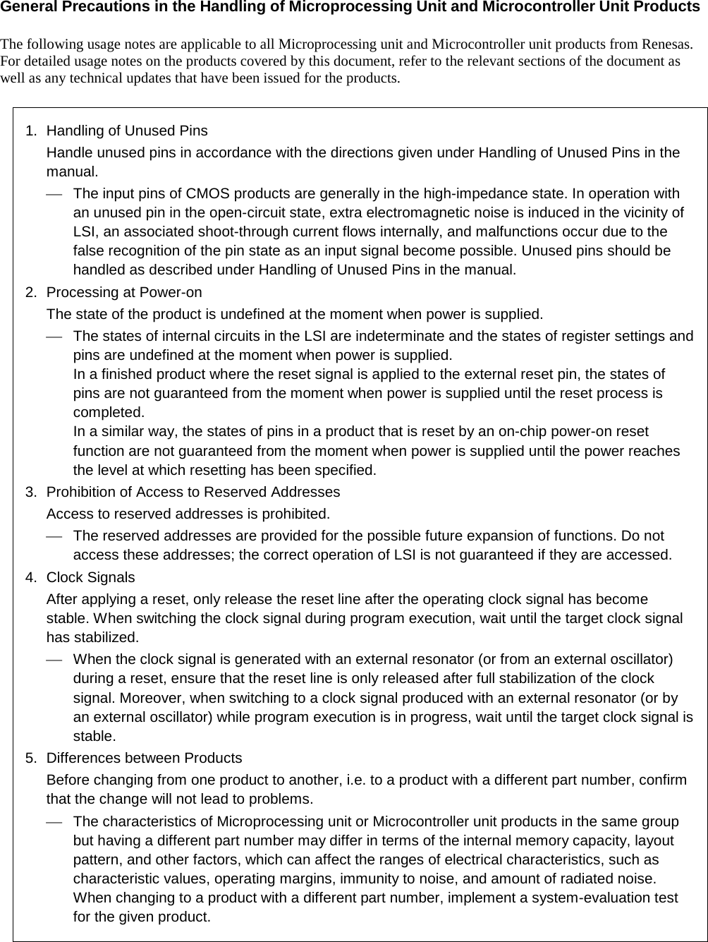
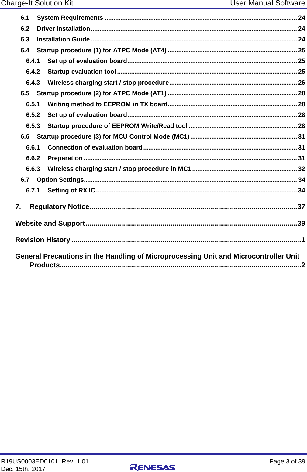
![Charge-It Solution Kit User Manual Software R19US0003ED0101 Rev. 1.01 Page 35 of 39 Dec. 15th, 2017 • Battery Protection Evaluation If “OFF” is selected, 2-wire serial communication interface is unavailable when battery protection is detected and DFET is off. If “ON” is selected for evaluation, DFET is NOT off when battery protection is detected, and 2-wire serial communication interface is available. • BUZ Mode Select notification action of BUZ pin when battery low voltage is detected. Refer to 0x34 D2 at register map. - LEVEL: Output low level - PULSE: Output pulse • DFET/Battery Protection setting Set Battery protection parameters. Refer to Table 10Input items of “WPT Communication setting”. • I2C Configuration setting Zero should be set. • CHG setting Set charge control profile for battery temperature. Set fast charge current, charge complete current, and constant voltage charge control voltage. Refer to Table 11. Table 9: Input items of “WPT Communication setting” Item RxIC Register Description WPT_T_RATE 0x27 D[1:0] WPT communication data rate setting. (Receiver to Transmitter communication) WPT_R_DIFF_WAIT 0x27 D[7:4] Timing to acquire the rectified output voltage variation for WPT communication packet demodulation. WPT_R_DIFF_OLD 0x27 D[3:2] Assigning data point to calculate the rectified output voltage variation for WPT communication packet demodulation. WPT_R_DIFF_TH 0x28 D[7:0] Threshold to detect the rectified output voltage variation for WPT communication packet demodulation. WPT_R_CNT_TH 0x29 D[7:0] Counter timing to detect data 0/1 for WPT communication packet demodulation. WPT_R_CNT_TH_1CYC 0x2A D[7:0] Counter timing to detect data presence/absence for WPT communication packet demodulation.](https://usermanual.wiki/Renesas-Electronics-Europe/CHARGE-IT/User-Guide-3753059-Page-35.png)
![Charge-It Solution Kit User Manual Software R19US0003ED0101 Rev. 1.01 Page 36 of 39 Dec. 15th, 2017 Table 10: Input items of “DFET/Battery protection setting” Item Description DFET SIZE Set DFET resistance. 0: 160m ohm, 1: 320m ohm, 2: 480m ohm, 3: 640m ohm DSCP Set discharge short circuit current detection level. 0: 100mV, 1: 120mV, 2: 140mV, 3: 160mV DOCP Set discharge overcurrent detection level 0: 50mV, 1: 60mV, 2: 70mV, 3: 80mV DOVP Set discharge overvoltage detection level 0: 2.8V, 1: 2.7V, 2: 2.9V, 3: 3.0V FG DETECTION Set battery low voltage detection level depending on DCDC converter output voltage. Value DCDC output voltage setting Detection level high Detection level low 0 1.2V,1.5V,1.8V 3.20V 3.05V 0 3.0V 3.55V 3.35V 1 1.2V,1.5V,1.8V 3.30V 3.15V 1 3.0V 3.65V 3.45V TJMAX Junction temperature detection level 0: 68[degC] 1: 79[degC] Table 11: Input items of “Charge Setting” Item RxIC Register Description ICC_THM_L 0x02 D[3:2] Fast charge current setting of low temperature operation in battery temperature profile. (1C / 0.5C / 0.25C) ICC_THM_M 0x02 D[5:4] Fast charge current setting of suitable temperature operation in battery temperature profile. (1C / 0.5C / 0.25C) ICC_THM_H 0x02 D[7:6] Fast charge current setting of high temperature operation in battery temperature profile. (1C /0.5C / 0.25C) ICV_FIN 0x03 D[1:0] Constant voltage charge complete current setting. (0.05C / 0.10C /0.15C /0.20C) VCV_THM_L 0x03 D[3:2] Constant voltage charge control voltage setting of low temperature operation in battery temperature profile. (4.05V / 4.20V / 4.35V) VCV_THM_M 0x03 D[5:4] Constant voltage charge control voltage setting of suitable temperature operation in battery temperature profile. (4.05V / 4.20V /4.35V) VCV_THM_H 0x03 D[7:6] Constant voltage charge control voltage setting of high temperature operation in battery temperature profile. (4.05V /4.20V /4.35V)](https://usermanual.wiki/Renesas-Electronics-Europe/CHARGE-IT/User-Guide-3753059-Page-36.png)