Shi Xinzhongxin Technology F-6688 Bluetooth Module User Manual www i enet com
Shenzhenshi Xinzhongxin Technology Co., Ltd. Bluetooth Module www i enet com
UserManual.wiki
>
Shi Xinzhongxin Technology
>
F 6688 User Manual
15_F-6688 UserMan, r1.pdf
Navigation menu
Upload a User Manual
Namespaces
Wiki Guide
HTML
PDF
Info
Views
User Manual
Discussion / Help
Navigation
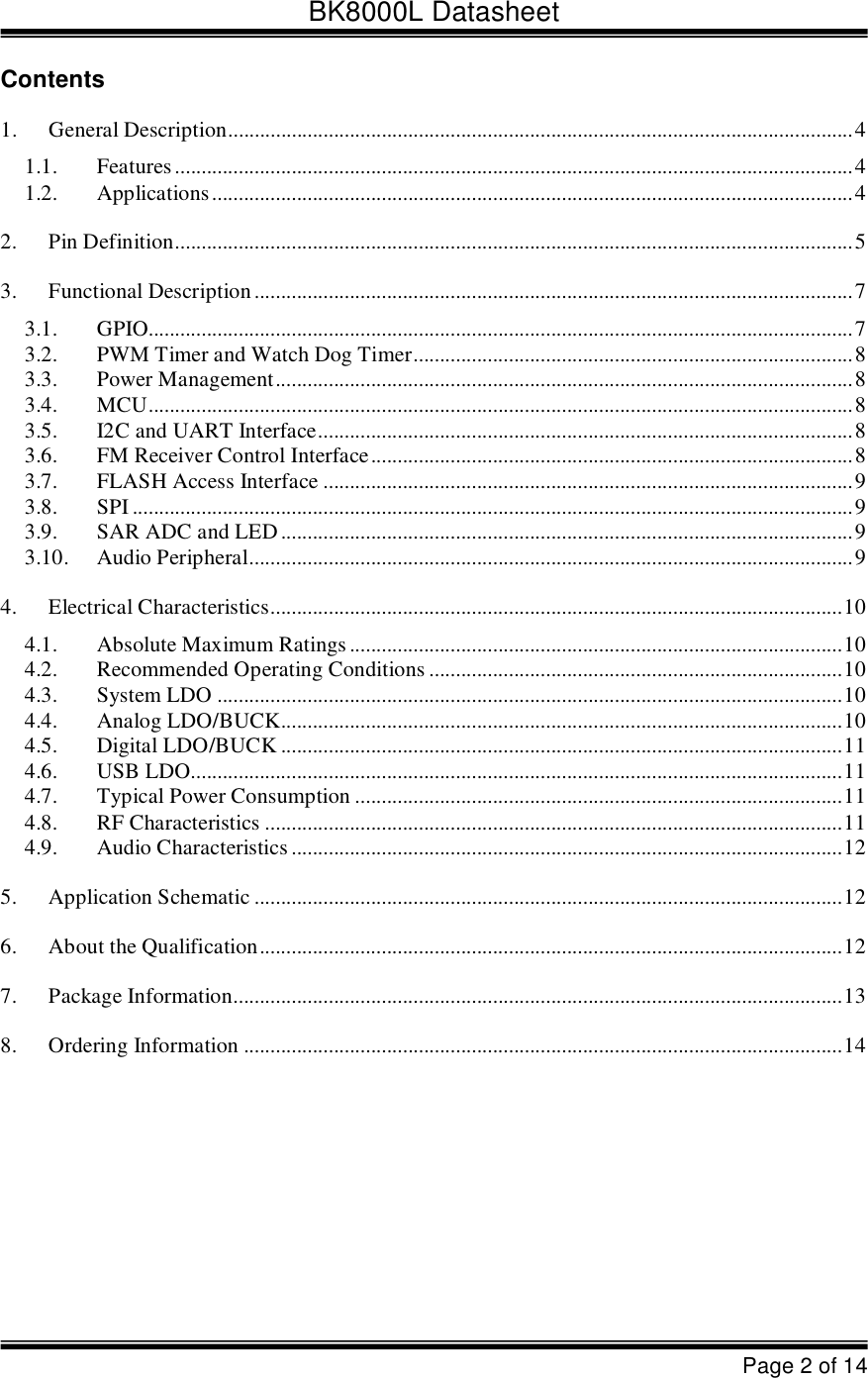
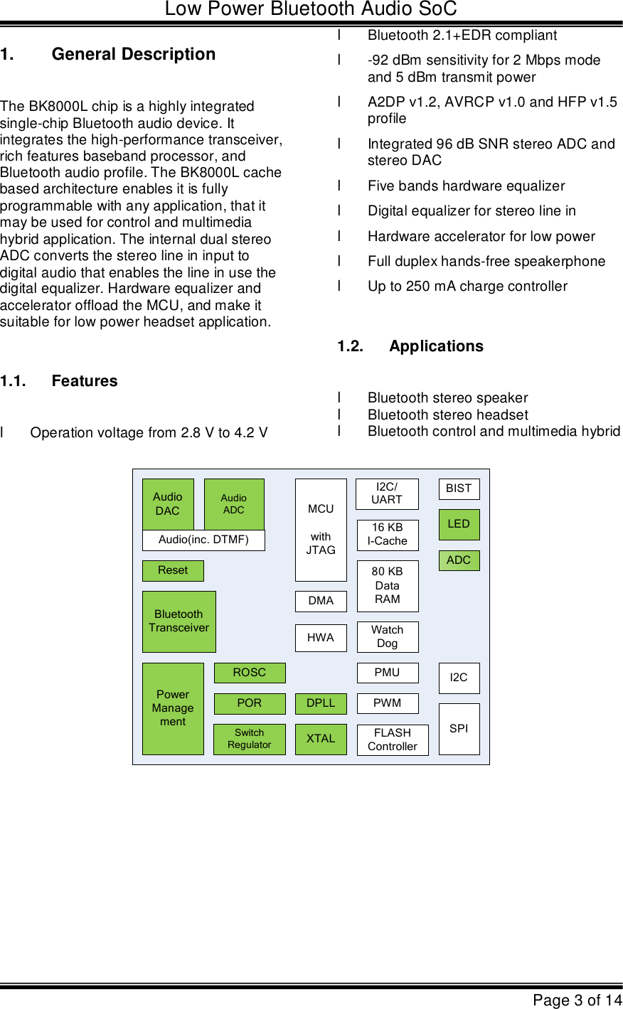
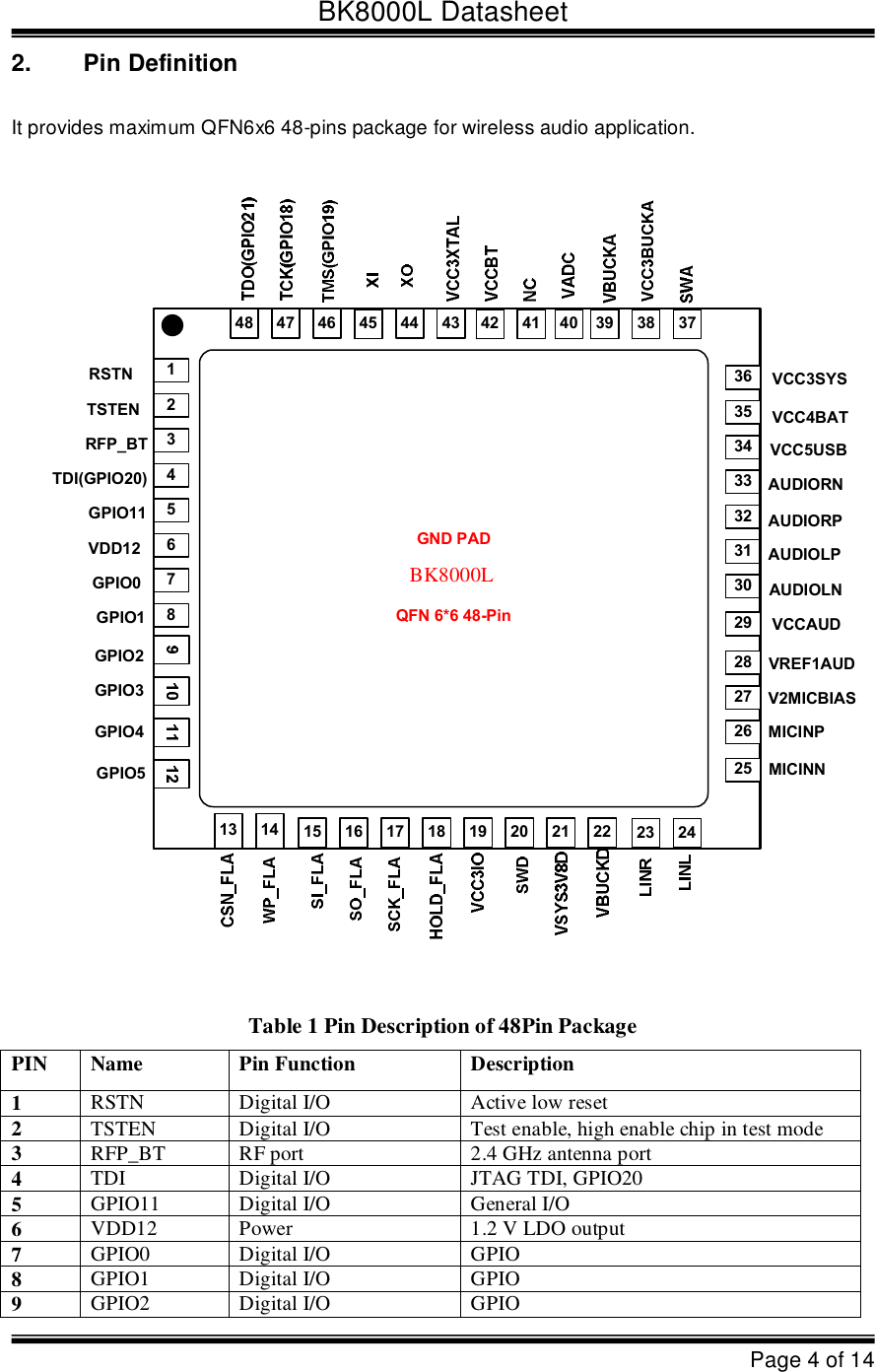
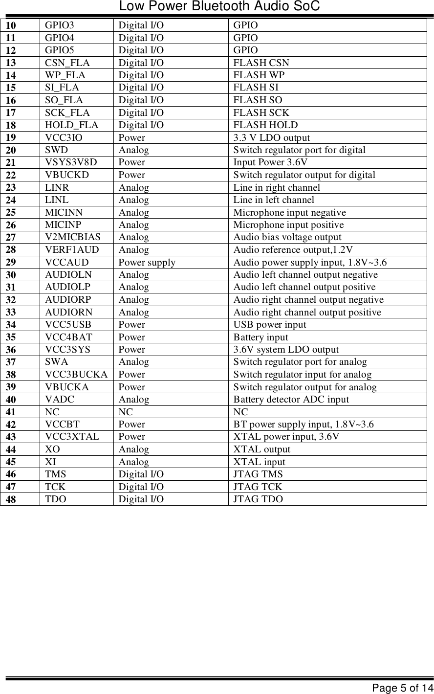
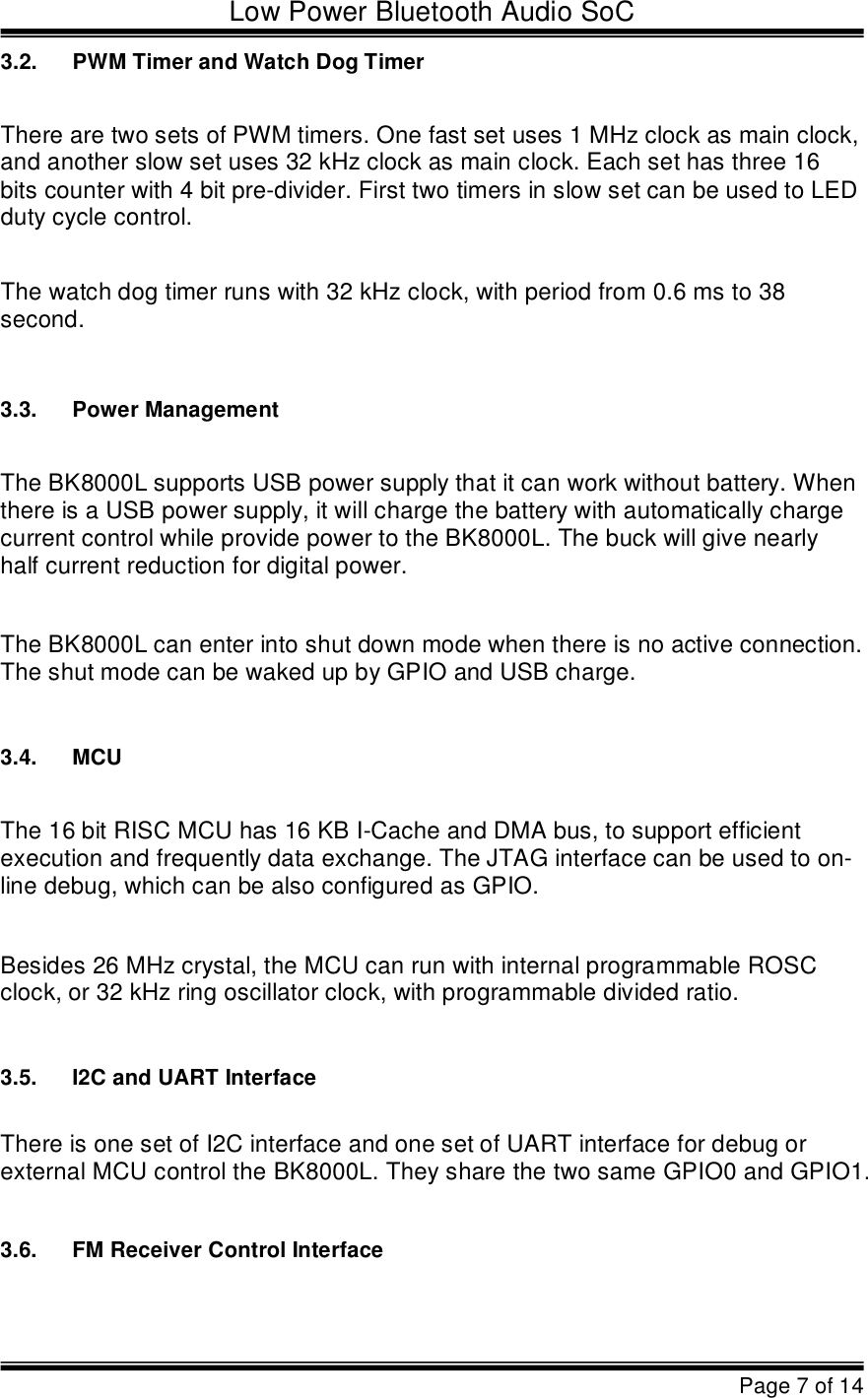
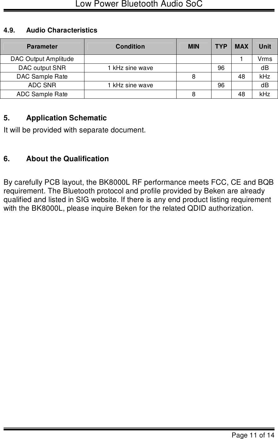
![BK8000L DatasheetPage 6 of 143.Functional Description3.1.GPIOThe BK8000L has total 19 GPIOs, which can be configured as either input or output. Most of them have second function. Table 2 GPIO Function MappingMbist ModePerial Mode GPIO ModeGPIO0Mbist DoneUART2_TXD/I2C2_SCLGeneral I/OGPIO1Mbist_FailUART2_RXD/I2C2_SDAGeneral I/OGPIO2inputpcm2_clk/TXENGeneral I/OGPIO3inputpcm2_sync/RXENGeneral I/OGPIO4inputpcm2_din/UART1_TX_MonitorGeneral I/OGPIO5inputpcm2_dout/UART1_RX_MonitorGeneral I/OGPIO6inputpcm2_codec_clk/spi_csnGeneral I/OGPIO7inputspi_sckGeneral I/OGPIO8inputspi_mosiGeneral I/OGPIO9inputspi_misoGeneral I/OGPIO10inputPWM0General I/OGPIO11Mbist_PassPWM1General I/OGPIO12inputsd_clk/clk13mGeneral I/OGPIO13inputsd_cmd/SCLGeneral I/OGPIO14inputsd_data[0]/SDAGeneral I/OGPIO15inputsd_data[1]General I/OGPIO16inputsd_data[2]General I/OGPIO17inputsd_data[3]General I/OGPIO18Mbist_Fail_BTjtag_TCKGeneral I/OGPIO19dram_result[2]jtag_TMSGeneral I/OGPIO20dram_result[1]jtag_TDI General I/OGPIO21dram_result[0]jtag_TDOGeneral I/OAll GPIO can be source to wake up MCU from shut down state. In shut down state, any level change on the set GPIO will trigger the wake up procedure. When power on, the default state of GPIO0~GPIO9 and GPIO12~GPIO20 is high impedance and pull low internally; the default state of GPIO10~GPIO11 is high impedance and pull high; and the default state of GPIO21 is high impedance only.](https://usermanual.wiki/Shi-Xinzhongxin-Technology/F-6688/User-Guide-2953775-Page-6.png)