Smart Approach MQN18-NFC NFC Antenna Module User Manual
Smart Approach Co., Ltd. NFC Antenna Module
UserManual.wiki
>
Smart Approach
>
MQN18 NFC User Manual
User manual
Navigation menu
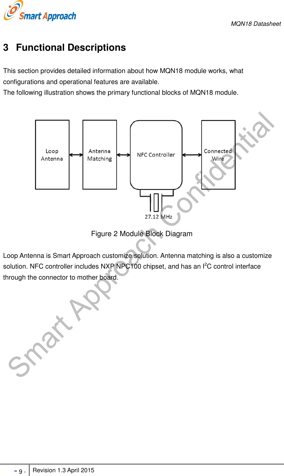
Upload a User Manual
Namespaces
Wiki Guide
HTML
PDF
Info
Views
User Manual
Discussion / Help
Navigation