Testo SE and KGaA AMB2520T 2.4 GHz Transceiver module User Manual manual 1
Testo AG 2.4 GHz Transceiver module manual 1
UserManual.wiki
>
Testo SE and KGaA
>
AMB2520T User Manual
>
manual 1
Contents
1.
manual 1
2.
manual 2
manual 1
Navigation menu
Upload a User Manual
Namespaces
Wiki Guide
HTML
PDF
Info
Views
User Manual
Discussion / Help
Navigation
![AMB8420/2520 Manual V3.6 Page 8 of 40 Last update: 25/3/2008 4.2 Power Consumption 4.2.1 AMB8420 See data sheet [4]. 4.2.2 AMB2520 See data sheet [5]. N.B.: To minimise power consumption in Sleep Mode, the input signals of the module (/CONFIG, SLEEP, TRX_DISABLE und /DATA_REQUEST) must be set to the levels defined in Table 2. Open (floating) pins result in increased power consumption. 5 Dimensions and Weight See data sheets [4] and [5].](https://usermanual.wiki/Testo-SE-and-KGaA/AMB2520T.manual-1/User-Guide-939157-Page-9.png)
![AMB8420/2520 Manual V3.6 Page 11 of 40 Last update: 25/3/2008 7 Serial Interface 7.1 UART 7.1.1 Supported Data Rates The data rate is adjusted by directly configuring the respective registers of the utilised microprocessor (see UART_TCTL, UART_MCTL, UART_BR0, and UART_BR1; from 12.1.1). In this way, the data rate can be adjusted freely from 0.5 to 115200 baud. As the UART speed is derived from the speed of the utilised clock quartz, there may be variations of up to 0.5%. When using the PC program "ACC", the following data rates can be selected directly via drop-down menu: 110, 300, 600, 1200, 2400, 4800, 9600, 14400, 19200, 28800, 38400, 56000, 57600, and 115200 baud. With this selection, the three registers above are automatically set to the optimum value. Moreover, the "ACC" program also provides a dialogue for calculating any baud rates. The default baud rate of the module is 9600 (AMB8420)/38400 (AMB2520). The output of characters on the serial interface takes place with secondary priority. For this reason, short interruptions may occur between the output of individual characters (e.g. in the event of an interrupt). 7.1.2 Supported Data Formats All data formats offered by the processor are supported: • 7 or 8 bits • No, even, or odd parity • 1 or 2 stop bits In ACC, the following data formats can be selected directly via the drop-down menu: 8n1, 8o1, 8e1, 8n2, 8o2, 8e2, 7n1, 7o1, 7e1, 7n2, 7o2, 7e2. The data format, too, can be set by directly configuring the respective microprocessor registers (see UART_CTL, 12.1.1). The default data format is 8 data bits, no parity, 1 stop bit ("8n1"). 7.2 SPI Interface Instead of the UART interface, the module also has an SPI interface. This interface is supported from software version 3.2 (separate firmware, can be installed with the Windows program "ACC"). See [6].](https://usermanual.wiki/Testo-SE-and-KGaA/AMB2520T.manual-1/User-Guide-939157-Page-12.png)
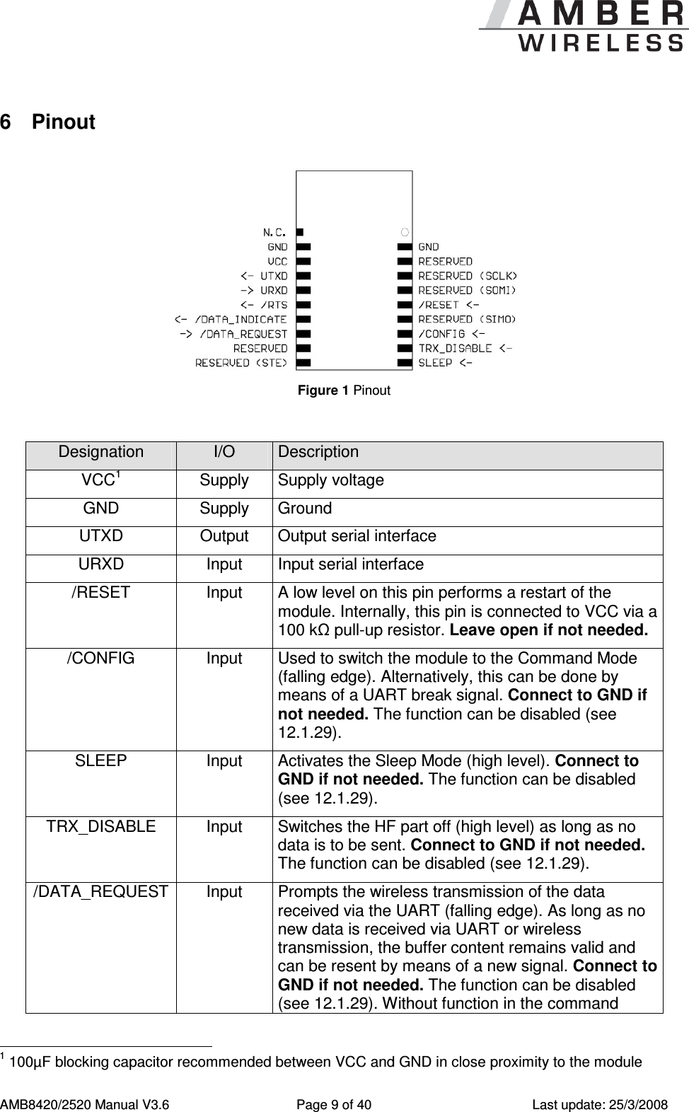
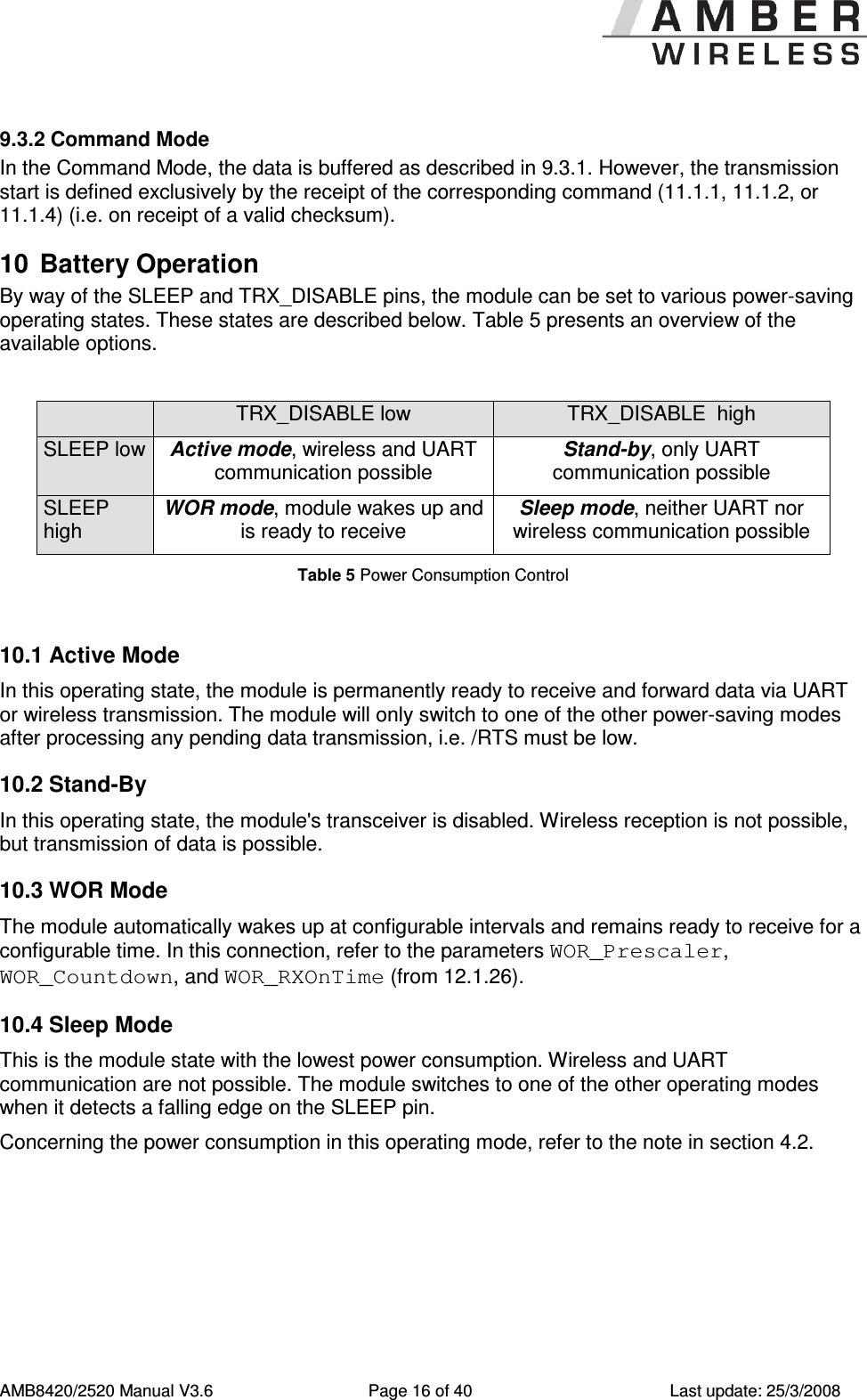
![AMB8420/2520 Manual V3.6 Page 13 of 40 Last update: 25/3/2008 8.2 AMB2520 In the factory state, the HF data rate is 250 kbps. The module AMB2520 uses a channel spacing of approximately 500 kHz; the carrier frequency can be determined with the following formula: )500.0(5.2400][ ⋅+=ChannelCNMHzF Here, the channels 0 to 165 are permissible. See Table 4 for an overview of usable frequencies. N.B.: Avoid the channels/frequencies (2405 MHz + n x 13MHz) marked in red, which merely provide a reduced range due to a property of the wireless IC. Channel no. Freq. [MHz] Channel no. Freq. [MHz] Channel no. Freq. [MHz] Channel no. Freq. [MHz] 0 2400.5 41 2421.0 82 2441.5 123 2462.0 1 2401.0 42 2421.5 83 2442.0 124 2462.5 2 2401.5 43 2422.0 84 2442.5 125 2463.0 3 2402.0 44 2422.5 85 2443.0 126 2463.5 4 2402.5 45 2423.0 86 2443.5 127 2464.0 5 2403.0 46 2423.5 87 2444.0 128 2464.5 6 2403.5 47 2424.0 88 2444.5 129 2465.0 7 2404.0 48 2424.5 89 2445.0 130 2465.5 8 2404.5 49 2425.0 90 2445.5 131 2466.0 9 2405.0 50 2425.5 91 2446.0 132 2466.5 10 2405.5 51 2426.0 92 2446.5 133 2467.0 11 2406.0 52 2426.5 93 2447.0 134 2467.5 12 2406.5 53 2427.0 94 2447.5 135 2468.0 13 2407.0 54 2427.5 95 2448.0 136 2468.5 14 2407.5 55 2428.0 96 2448.5 137 2469.0 15 2408.0 56 2428.5 97 2449.0 138 2469.5 16 2408.5 57 2429.0 98 2449.5 139 2470.0 17 2409.0 58 2429.5 99 2450.0 140 2470.5 18 2409.5 59 2430.0 100 2450.5 141 2471.0 19 2410.0 60 2430.5 101 2451.0 142 2471.5 20 2410.5 61 2431.0 102 2451.5 143 2472.0 21 2411.0 62 2431.5 103 2452.0 144 2472.5 22 2411.5 63 2432.0 104 2452.5 145 2473.0 23 2412.0 64 2432.5 105 2453.0 146 2473.5 24 2412.5 65 2433.0 106 2453.5 147 2474.0 25 2413.0 66 2433.5 107 2454.0 148 2474.5 26 2413.5 67 2434.0 108 2454.5 149 2475.0 27 2414.0 68 2434.5 109 2455.0 150 2475.5 28 2414.5 69 2435.0 110 2455.5 151 2476.0](https://usermanual.wiki/Testo-SE-and-KGaA/AMB2520T.manual-1/User-Guide-939157-Page-14.png)
![AMB8420/2520 Manual V3.6 Page 14 of 40 Last update: 25/3/2008 Channel no. Freq. [MHz] Channel no. Freq. [MHz] Channel no. Freq. [MHz] Channel no. Freq. [MHz] 29 2415.0 70 2435.5 111 2456.0 152 2476.5 30 2415.5 71 2436.0 112 2456.5 153 2477.0 31 2416.0 72 2436.5 113 2457.0 154 2477.5 32 2416.5 73 2437.0 114 2457.5 155 2478.0 33 2417.0 74 2437.5 115 2458.0 156 2478.5 34 2417.5 75 2438.0 116 2458.5 157 2479.0 35 2418.0 76 2438.5 117 2459.0 158 2479.5 36 2418.5 77 2439.0 118 2459.5 159 2480.0 37 2419.0 78 2439.5 119 2460.0 160 2480.5 38 2419.5 79 2440.0 120 2460.5 161 2481.0 39 2420.0 80 2440.5 121 2461.0 162 2481.5 40 2420.5 81 2441.0 122 2461.5 163 2482.0 164 2482.5 165 2483.0 Table 4 Frequency assignment AMB2520 9 Timing Parameters 9.1 Reset Behaviour Following a reset, a low level on the /RTS pin signals that the module is ready for operation. However, the level is only valid after the time required for the internal initialisation of the processor (a couple of µs). After this initialisation, /RTS is first set to high. Then the processor rate is calibrated on the basis of the watch crystal. Only after this procedure is the module ready for operation. 9.1.1 Power-On Reset After setting the supply voltage and releasing the /RESET pin (if wired), the period until the module is ready for operation greatly depends on the build time of the clock quartz. This procedure may take up to 1 second; typical values range from 200 to 400 ms. Recommended procedure: Check for low level on /RTS pin 2 ms after setting the prescribed supply voltage. Subsequently, an additional 100 µs is required until readiness. 9.1.2 Reset via /RESET Pin To force a module restart by means of the /RESET pin, it must first be set to low for at least 10 ms. After the pin is released, /RTS will switch to high after 100 µs at the latest. As the build-up time for the clock quartz does not apply in this case, the time until the module is ready for operation is reduced to a couple of ms. During this time, the processor rate will be calibrated, which takes anywhere between 2 and 20 ms depending on the supply voltage and temperature. Recommended procedure: After the /RESET pin is released, wait for 2 ms for low level on the /RTS pin. Subsequently, an additional 100 µs are required until readiness.](https://usermanual.wiki/Testo-SE-and-KGaA/AMB2520T.manual-1/User-Guide-939157-Page-15.png)
![AMB8420/2520 Manual V3.6 Page 23 of 40 Last update: 25/3/2008 11.10 CMD_RSSI_REQ This command delivers the current RX level determined by the transceiver IC in the form of a two's complement. Format: 0x02 0x0D 0x00 0x0F Return: 0x02 0x4D 0x01 < RX level > < CS > The value obtained in this way delivers the RX level RSSIdBm in dBm as follows: 1. Conversion of the hexadecimal value to a decimal RSSIdec 2. If RSSIdec ≥ 128: RSSIdBm = (RSSIdec –256) / 2 - RSSIOffset 3. Otherwise (RSSIdec < 128): RSSIdBm = RSSIdec / 2 - RSSIOffset RSSIOffset is a data-rate-dependent correction factor according to Table 6 (AMB8420) and Table 7 (AMB2520). The relation between the calculated value and the physical RX level in dBm is not linear across the entire operating range and is displayed in Figure 2 and Figure 3 . Data rate RSSI offset 1.2 kbps 74 38.4 kbps 74 250 kbps 78 Table 6 Data rate-dependent RSSI offset for AMB8420 (from [2]) Data rate RSSI offset 2.4 kbps 71 10 kbps 69 250 kbps 72 500 kbps 72 Table 7 Data rate-dependent RSSI offset for AMB2520 (from [3])](https://usermanual.wiki/Testo-SE-and-KGaA/AMB2520T.manual-1/User-Guide-939157-Page-24.png)
![AMB8420/2520 Manual V3.6 Page 24 of 40 Last update: 25/3/2008 Figure 2 Relation between the RX level and the RSSI value read out for AMB8420 (from [2]) Figure 3 Relation between the RX level and the RSSI value read out for AMB2520 (from [3])](https://usermanual.wiki/Testo-SE-and-KGaA/AMB2520T.manual-1/User-Guide-939157-Page-25.png)
![AMB8420/2520 Manual V3.6 Page 25 of 40 Last update: 25/3/2008 11.11 CMD_ERRORFLAGS_REQ This command returns internal error states. Format: 0x02 0x0E 0x00 0x0C Return: 0x02 0x4E 0x02 < error flags MSB > < error flags LSB >< CS > An error flag return value of "0" indicates that no error has occurred. The value is set back after the query and in the event of a reset. The meaning of the error flags is not described in detail in this context. 12 Configuration Parameters 12.1 Non-Volatile Configuration Parameters The non-volatile parameters listed in the following table can be modified by means of specific commands in the configuration mode (CMD_SET_REQUEST, see 11.7) of the module or by using the Windows software "ACC". These parameters are stored permanently in the module's flash memory. Caution: The validity of the specified parameters is not verified. Incorrect values can result in device malfunction! Designation Designation in ACC Summary Permissible values Default AMB8420 / AMB2520 Memory position Number of bytes UART_CTL Data format Control register for UART data format See Table 9 16 0 1 UART_TCTL Control register for the baud rate (change only after consultation) 32 32 1 1 UART_MCTL MCTL Control register for fine-adjusting the UART baud rate; concerning the calculation, see [1] 0 - 255 0 / 68 2 1 UART_BR0 BR0 Prescaler for setting the baud rate (LSB); concerning the calculation, see [1] 0 - 255 113 / 156 3 1 UART_BR1 BR1 Prescaler for setting the baud rate (MSB); concerning the 0 - 255 2 / 0 4 1](https://usermanual.wiki/Testo-SE-and-KGaA/AMB2520T.manual-1/User-Guide-939157-Page-26.png)
![AMB8420/2520 Manual V3.6 Page 26 of 40 Last update: 25/3/2008 Designation Designation in ACC Summary Permissible values Default AMB8420 / AMB2520 Memory position Number of bytes calculation, see [1] UART_PktMode Packetizing mode Selects the packet generation method 0 or 1 0 5 1 UART_PktSize Packet size Number of characters for transmission start with set packet size 1 - 128 128 7 1 UART_RTSLimit /RTS limit Number of received characters after which /RTS responds 1 - 128 112 8 1 UART_ETXChar ETX character End-of-text character used to mark data packets; reception of this character triggers wireless transmission 0 - 255 10 9 1 UART_Timeout Timeout Timeout after the last character before the data received via UART are transmitted via wireless transmission (in milliseconds) 0 – 65535 5 12 2 UART_DIDelay Data indication delay Delay between the signalling by the /DATA_INDICATION pin and the start of the output via UART 0 – 65535 0 14 2 MAC_NumRetrys Retrys Number of wireless retries 0 – 255 0 20 1 MAC_AddrMode Addressing mode Addressing mode to use 0/1/2 0 21 1 MAC_DestNetID Dest. net ID Default destination network ID 0 – 255 0 24 1 MAC_DestAddrLSB Dest. device address Default destination address (LSB) 0 – 255 0 25 1 MAC_SourceNetID Local net ID Own network ID 0 – 254 0 28 1 MAC_SourceAddrLSB Local device address Own address (LSB) 0 – 254 0 29 1 MAC_ACKTimeout ACK timeout Waiting time for wireless acknowledgement in 0 – 65535 10 32 2](https://usermanual.wiki/Testo-SE-and-KGaA/AMB2520T.manual-1/User-Guide-939157-Page-27.png)
![AMB8420/2520 Manual V3.6 Page 28 of 40 Last update: 25/3/2008 Designation Designation in ACC Summary Permissible values Default AMB8420 / AMB2520 Memory position Number of bytes 12.1.29 Synch1 Synch1 Synch word MSB for transceiver (change only after consultation!) 0 - 255 211 76 1 Synch0 Synch0 Synch word LSB for transceiver (change only after consultation) 0 - 255 145 77 1 Table 8 Overview of Non-Volatile Configuration Parameters 12.1.1 UART_CTL The UART data format can be configured with the help of the upper 4 bits in this register. The meaning of these bits is described in Table 9. Bit no. Description 0 to 3 (0x0F) Reserved, must always be set to 0. 4 (0x10) If this bit is set, the character length will be 8 bits, if not, it will be 7 bits. 5 (0x20) This bit selects the number of stop bits. If this bit is set, 2 stop bits will be used, if not, 1 will be used. 6 (0x40) If this bit is set, even parity will be used, if not, odd parity will be used. 7 (0x80) This bit enables the use of parity (if set). Table 9 Setting the Data Format 12.1.2 UART_TCTL This register selects the source for generating the UART clock speed. Currently, the only permissible value is 32. 12.1.3 UART_MCTL The registers UART_MCTL, UART_BR0, and UART_BR1 can be used to set the UART baud rate. Concerning the calculation of the corresponding settings, see [1]. 12.1.4 UART_BR0 The registers UART_MCTL, UART_BR0, and UART_BR1 can be used to set the UART baud rate. Concerning the calculation of the corresponding settings, see [1].](https://usermanual.wiki/Testo-SE-and-KGaA/AMB2520T.manual-1/User-Guide-939157-Page-29.png)
![AMB8420/2520 Manual V3.6 Page 29 of 40 Last update: 25/3/2008 12.1.5 UART_BR1 The registers UART_MCTL, UART_BR0, and UART_BR1 can be used to set the UART baud rate. Concerning the calculation of the corresponding settings, see [1] 12.1.6 UART_PktMode Selects the method used for generating packets for the transparent operating mode. Two methods have been implemented: 0. Mode 0: Sends when a. the timeout defined with UART_Timeout is reached, or b. the number of bytes defined with UART_PktSize is reached, or c. the transmission of the data is requested by means of the /DATA_REQUEST pin. 1. Mode 1: Sends when a. the character defined with UART_ETXChar is detected, or b. the number of bytes defined with UART_PktSize has been received, or c. the transmission of the data is requested by means of the /DATA_REQUEST pin. 12.1.7 UART_PktSize Maximum number of bytes after which the wireless transmission of the data received via UART starts. Used in packet mode 0 as well as in packet mode 1. Not used in the command mode. 12.1.8 UART_RTSLimit Number of bytes after which the host system is prompted to interrupt the data transfer over /RTS. Necessary, because an immediate response to the /RTS signal may not take place (UART FIFO), depending on the host system. 12.1.9 UART_ETXChar End-of-text character that triggers the transmission of the data received via UART. Only used in packet mode 1. During the wireless transmission, the ETX character is treated like a normal character. Not used in the Command Mode. 12.1.10 UART_Timeout Timeout in milliseconds after the last character has been received on UART before the wireless transmission of the data received via UART starts. Only used in packet mode 0. If no new character is detected for this period after the STX character has been received in the command mode, the characters received until then will be dropped, and the unit will wait for a new start character. Not used in the Command Mode.](https://usermanual.wiki/Testo-SE-and-KGaA/AMB2520T.manual-1/User-Guide-939157-Page-30.png)
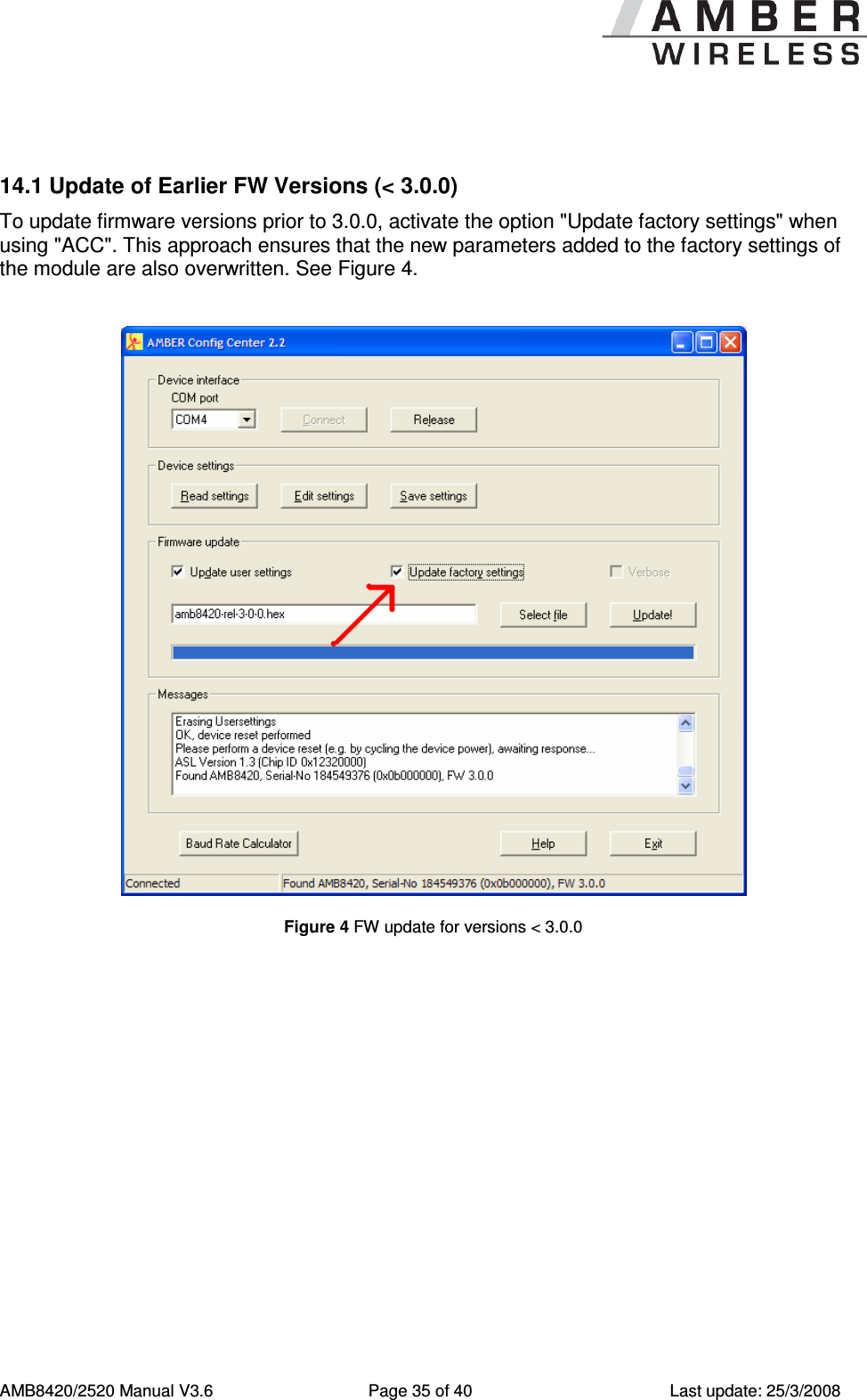
![AMB8420/2520 Manual V3.6 Page 38 of 40 Last update: 25/3/2008 16 Version History 16.1 Software Version 3.0 • Product release Version 3.1 • Bug fix "break detection" Version 3.2 • Bug fix UART_DIDelay in Command Mode • Sniffer mode via CfgFlags • SPI variant available 16.2 Manual Version 3.6 (valid for software versions 3.0, 3.1, and 3.2) • Clarification of packet formation in Command Mode (also concerns /DATA_REQUEST) • Readout of the RSSI value: added specification for AMB2520 • Added electrical parameters AMB2520 • Switching to the Command Mode only with delay after /RTS low (2.2.1) • Added timing parameters • Added restrictions for channel table AMB2520 17 References [1] To calculate the baud rate registers UART_MCTL, UART_BR0, and UART_BR1, the "Baud Rate Calculator" tool is integrated in ACC. To configure a standard baud rate, ACC provides a drop-down field with automatic calculation and parameterisation of the baud rate registers. [2] "CC1100 Single-Chip Low-Cost Low-Power RF Transceiver (Rev. B)", Texas Instruments [3] "CC2500 Single-Chip Low-Cost Low-Power RF Transceiver (Rev. B)", Texas Instruments [4] "AMB8420 Data Sheet", AMBER wireless GmbH [5] "AMB2520 Data Sheet", AMBER wireless GmbH [6] "AMB8420 / AMB2520 SPI Operation" AMBER wireless GmbH](https://usermanual.wiki/Testo-SE-and-KGaA/AMB2520T.manual-1/User-Guide-939157-Page-39.png)