Unigen UGWANBL2 Bluetooth Low Energy Module User Manual
Unigen Corporation Bluetooth Low Energy Module
UserManual.wiki
>
Unigen
>
UGWANBL2 User Manual
user manual
Navigation menu
Upload a User Manual
Namespaces
Wiki Guide
HTML
PDF
Info
Views
User Manual
Discussion / Help
Navigation
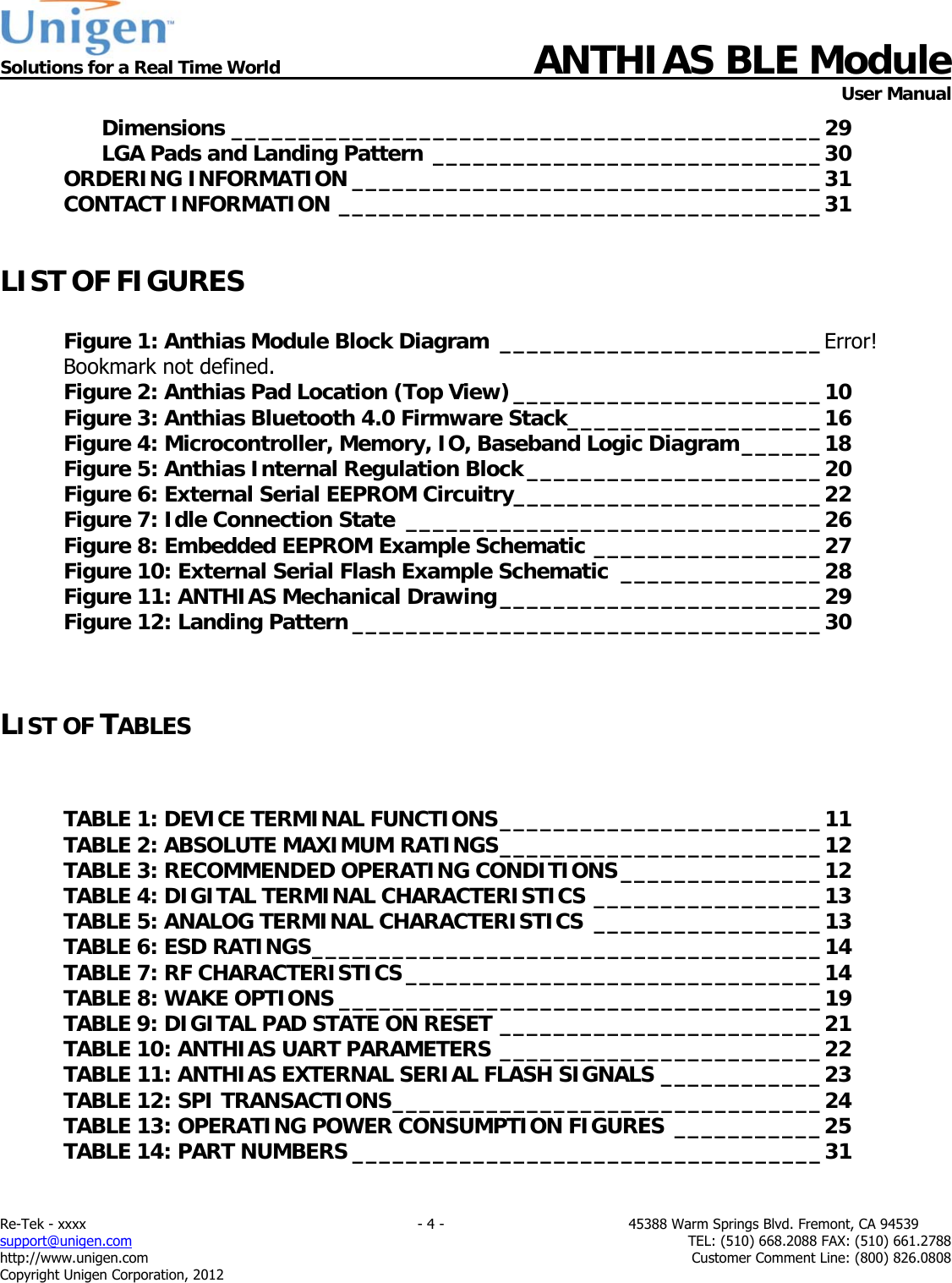
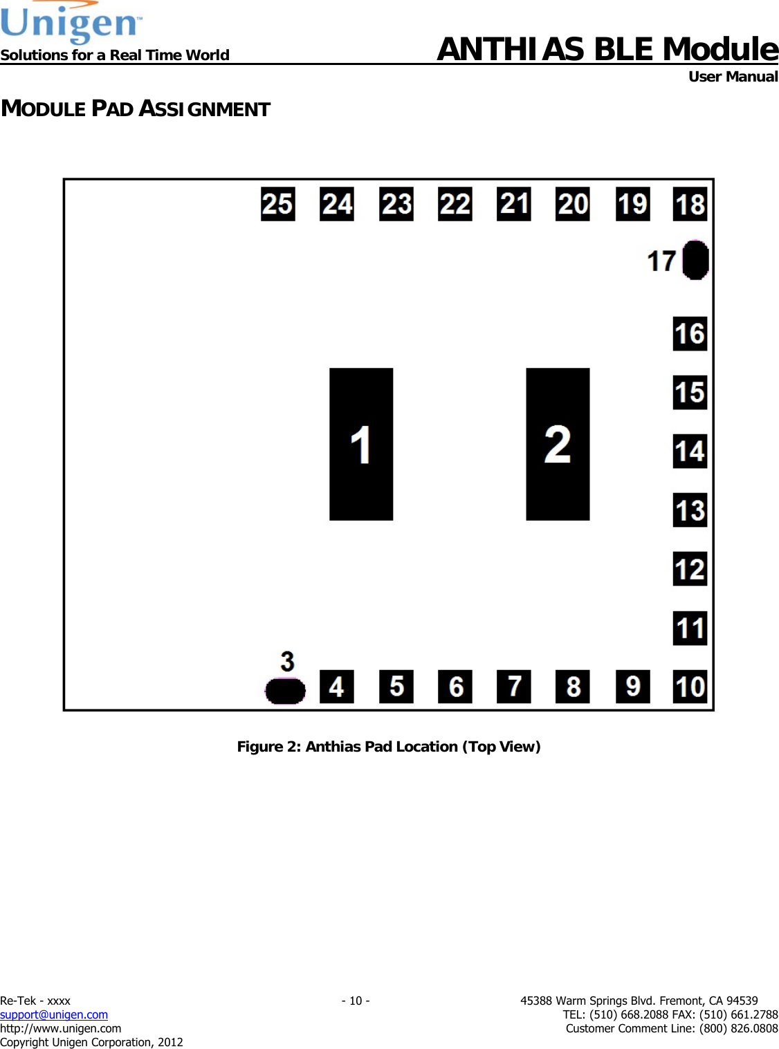
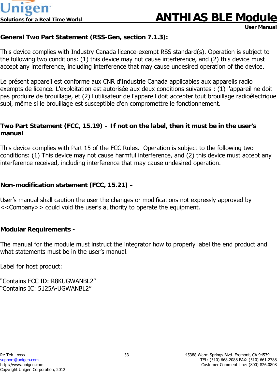
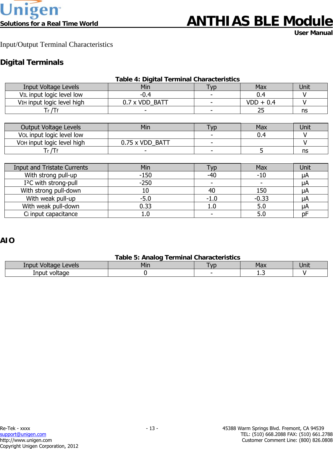
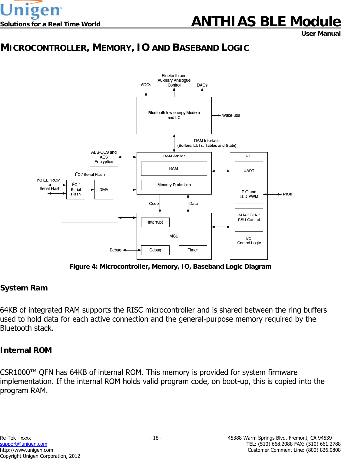
![Solutions for a Real Time World ANTHIAS BLE Module User Manual Re-Tek - xxxx - 11 - 45388 Warm Springs Blvd. Fremont, CA 94539 support@unigen.com TEL: (510) 668.2088 FAX: (510) 661.2788 http://www.unigen.com Customer Comment Line: (800) 826.0808 Copyright Unigen Corporation, 2012 DEVICE TERMINAL FUNCTIONS Table 1: Device Terminal Functions PAD Pad Type Label Description 1,2,25 - GND Module Ground 3,17 - NC Not Connected 4 Bidirectional analog AIO_2 Analogue programmable I/O line 5 AIO_1 6 AIO_0 7 Bidirectional with Programmable strength internal pullup/down PIO_0 / UART_TX Programmable I/O line or UART TX. 8 PIO_1 / UART_RX Programmable I/O line or UART RX. 9 PIO_3 / SF_DIN Programmable I/O line or SPI serial flash data (SF_DIN) input 10 PIO_4 / SF_CS# Programmable I/O line or SPI serial flash chip select (SF_CS#) 11 PIO_5 / SPI_CLK Programmable I/O line or DEBUG_CLK selected by SPI_PIO# 12 PIO_6 / SPI_CS# Programmable I/O line or DEBUG_CS# selected by SPI_PIO# 13 PIO_7 / SPI_MOSI Programmable I/O line or DEBUG_MOSI selected by PI_PIO# 14 PIO_8 / SPI_MISO Programmable I/O line or DEBUG_MISO selected by SPI_PIO# 15 PIO_9 Programmable I/O line 16 PIO_10 Programmable I/O line 18 Bidirectional Programmable strength internal pullup/down PIO_11 Programmable I/O line. 19 Input strong internal pull-down SPI_PIO#_SEL Selects SPI debug on PIO[8:5] 20 Bidirectional, tristate, weak internal pull-up I2C_SDA / SF_DOUT SPI serial flash data output; SF_DOUT 21 Input with weak internal pull-up I2C_SCL / SF_CLK SPI serial flash clock output; SF_CLK 22 Bidirectional with programmable strength internal pullup/down PIO_2 / I2C_SF_VDD Programmable I/O line or I²C Serial Flash power supply 23 - VDD_BAT 3V Power from supply or battery input 24 Input has no internal pull-up or pull-down, use external pulldown. WAKE Input to wake the module from hibernate](https://usermanual.wiki/Unigen/UGWANBL2/User-Guide-1828523-Page-11.png)

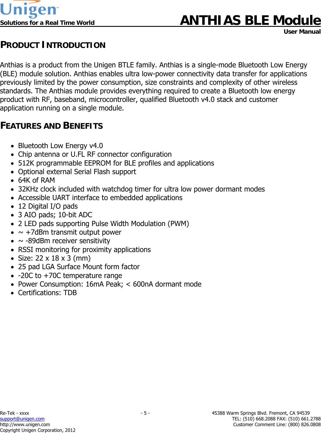
![Solutions for a Real Time World ANTHIAS BLE Module User Manual Re-Tek - xxxx - 19 - 45388 Warm Springs Blvd. Fremont, CA 94539 support@unigen.com TEL: (510) 668.2088 FAX: (510) 661.2788 http://www.unigen.com Customer Comment Line: (800) 826.0808 Copyright Unigen Corporation, 2012 Microcontroller The microcontroller, interrupt controller and event timer execute the Bluetooth Low Energy software stack and control the BLE radio and external interfaces. A 16-bit RISC microcontroller is used for low power consumption and efficient use of memory. Programmable I/O Ports, PIO and AIO 12 lines of programmable bidirectional I/O are provided. They are all powered from the Anthias internal regulating circuitry. PIO lines are software-configurable as weak pull-up, weak pull-down, strong pull-up or strong pull-down. Note: At reset all PIO lines are inputs with internal weak pull-downs. Any of the PIO lines can be configured as interrupt request lines or to wake the module from deep sleep mode. Table below lists the options for waking the module from the sleep modes. Table 8: Wake Options Sleep Mode Wake-up Options Dormant Can only be woken by the WAKE pad. Hibernate Can only be woken by the WAKE pad or by the watchdog timer. Deep Sleep Can be woken by any PIO configured to wake the module. The Anthias module supports alternative functions on the PIO lines: SPI Interface UART LED Flasher / PWM modules Note: Unigen cannot guarantee that all the PIO assignments remain as described. Implementation of the PIO lines is firmware build specific. For more information, see relevant software release note. Anthias has 3 general purpose analog interface pads, AIO[2:0] .](https://usermanual.wiki/Unigen/UGWANBL2/User-Guide-1828523-Page-19.png)
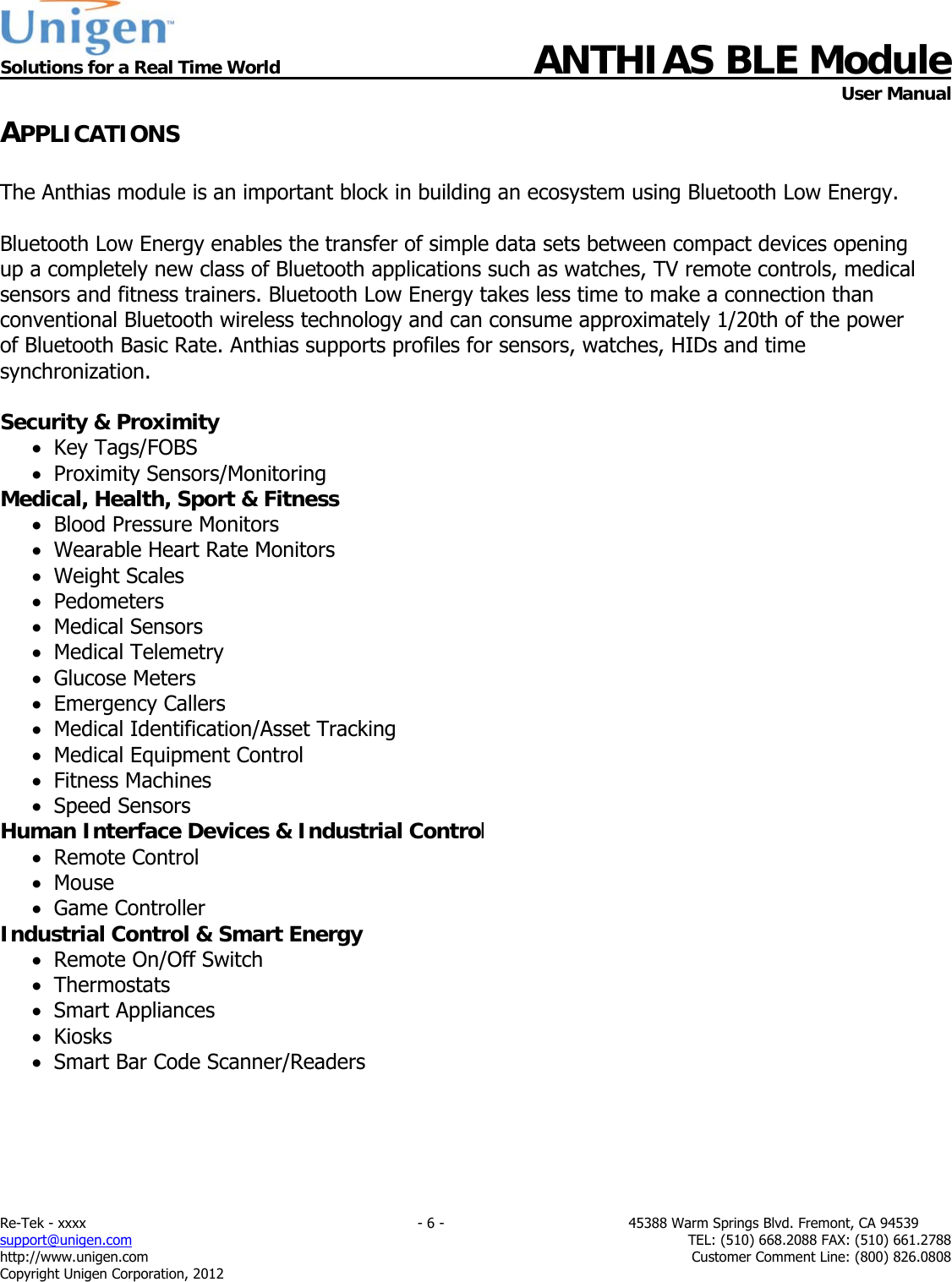
![Solutions for a Real Time World ANTHIAS BLE Module User Manual Re-Tek - xxxx - 21 - 45388 Warm Springs Blvd. Fremont, CA 94539 support@unigen.com TEL: (510) 668.2088 FAX: (510) 661.2788 http://www.unigen.com Customer Comment Line: (800) 826.0808 Copyright Unigen Corporation, 2012 Reset Anthias is reset by software-configured watchdog timer. Digital Pad States on Reset Table 9: Digital Pad State on Reset Pad Name / Group On Reset I2C_SDA Strong PU I2C_SCL Strong PU PIO[11:0] Weak PD SERIAL INTERFACES Application UART Interface The Anthias UART interface provides a simple mechanism for communicating with other serial devices using the RS232 protocol. 2 signals implement the UART function, UART_TX and UART_RX. When Anthias is connected to another digital device, UART_RX and UART_TX transfer data between the 2 devices. UART configuration parameters, e.g. baud rate and data format, are set using ANTHIAS application code firmware. When selected in firmware PIO[0] is assigned to a UART_TX output and PIO[1] is assigned to a UART_RX input, see the module pad assignment and description for more details. The UART CTS and UART RTS signals can be assigned to any PIO pad by the on-chip firmware. Note: To communicate with the UART at its maximum data rate using a standard PC, the PC requires an accelerated serial port adapter card.](https://usermanual.wiki/Unigen/UGWANBL2/User-Guide-1828523-Page-21.png)
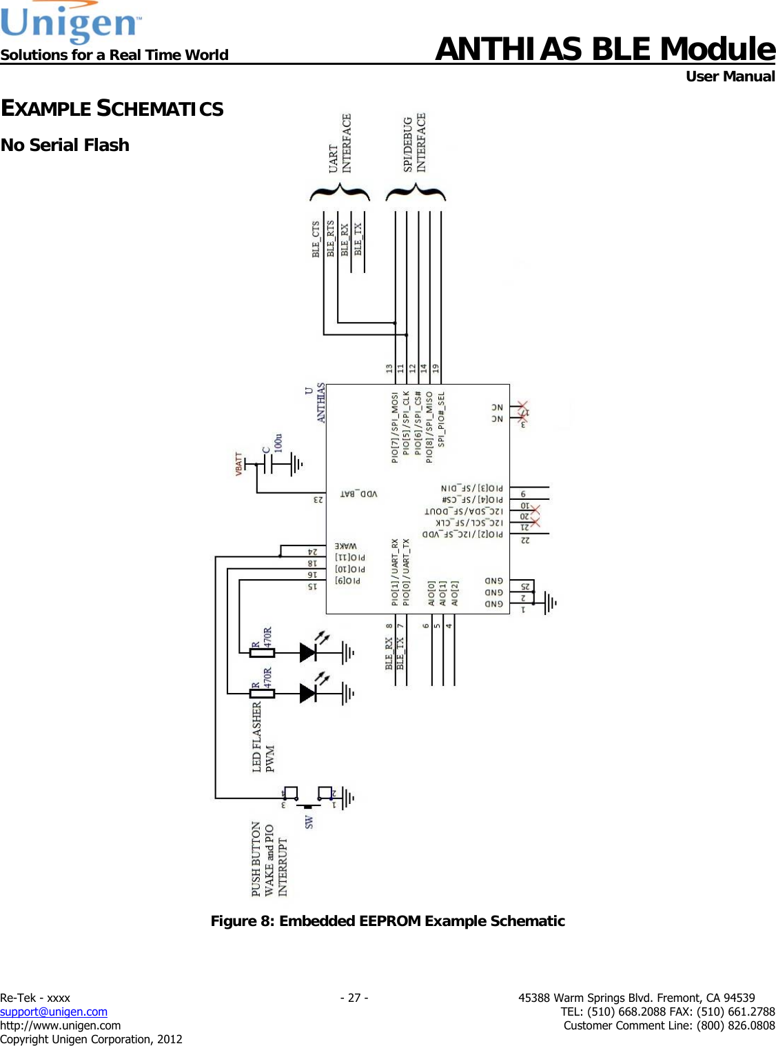
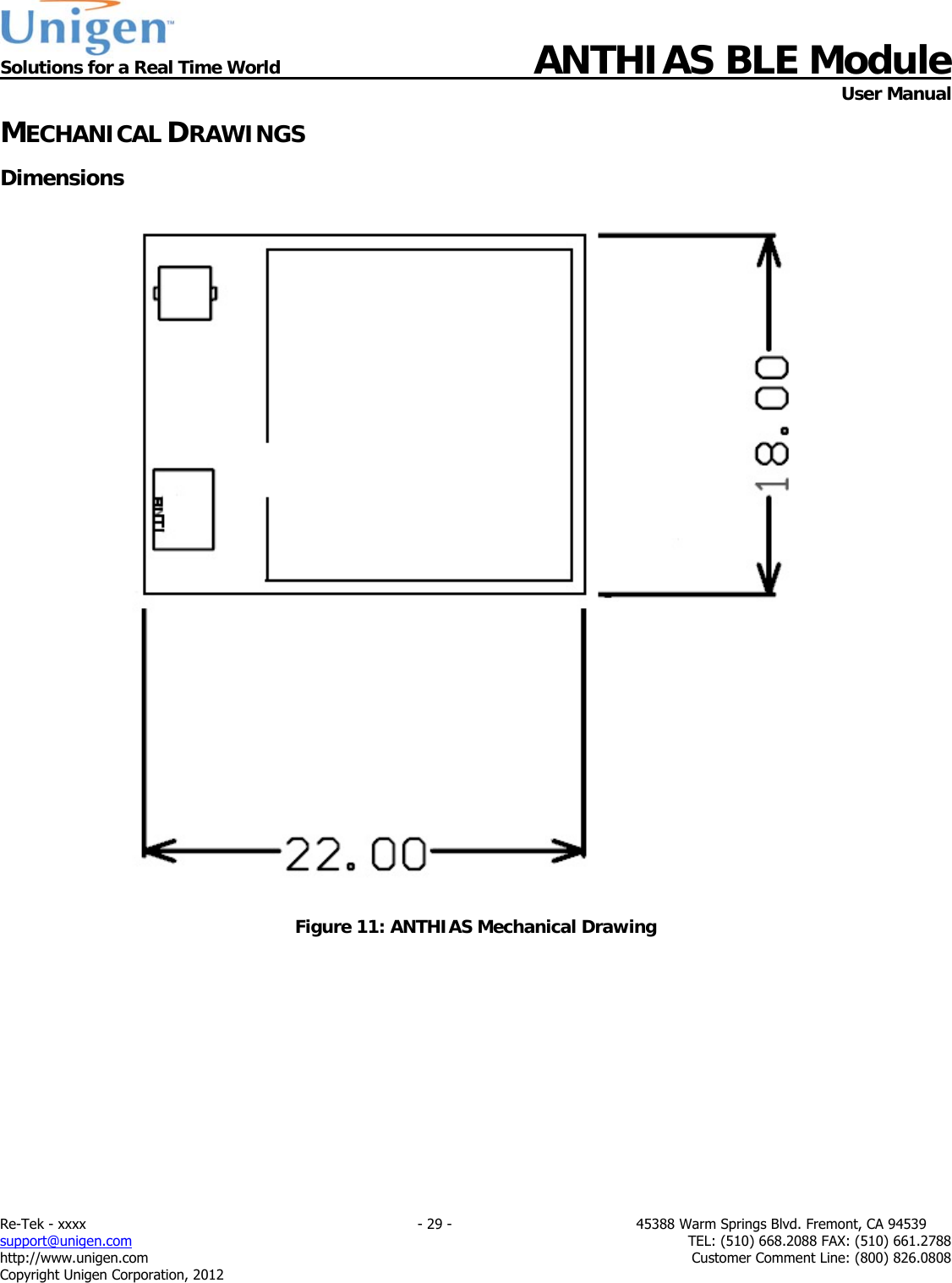
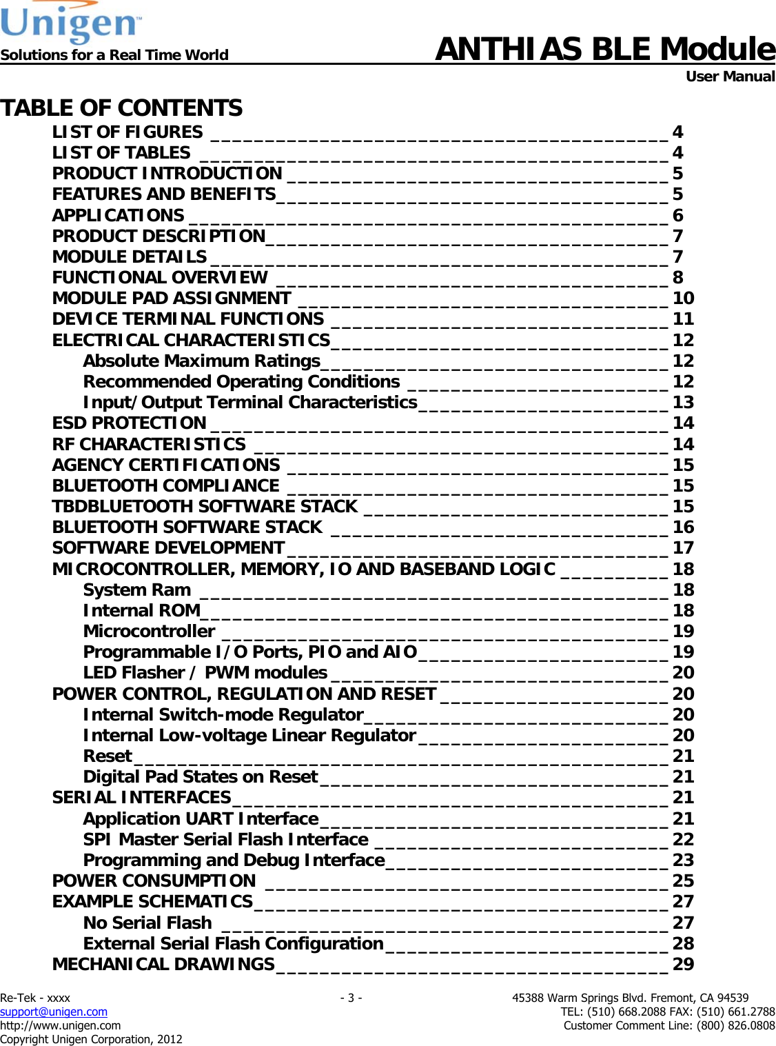
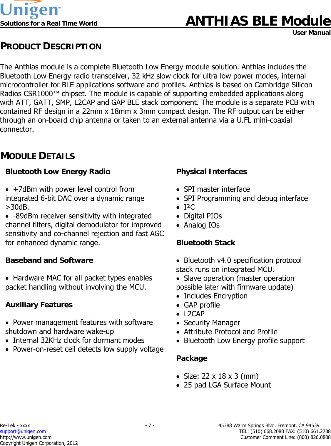
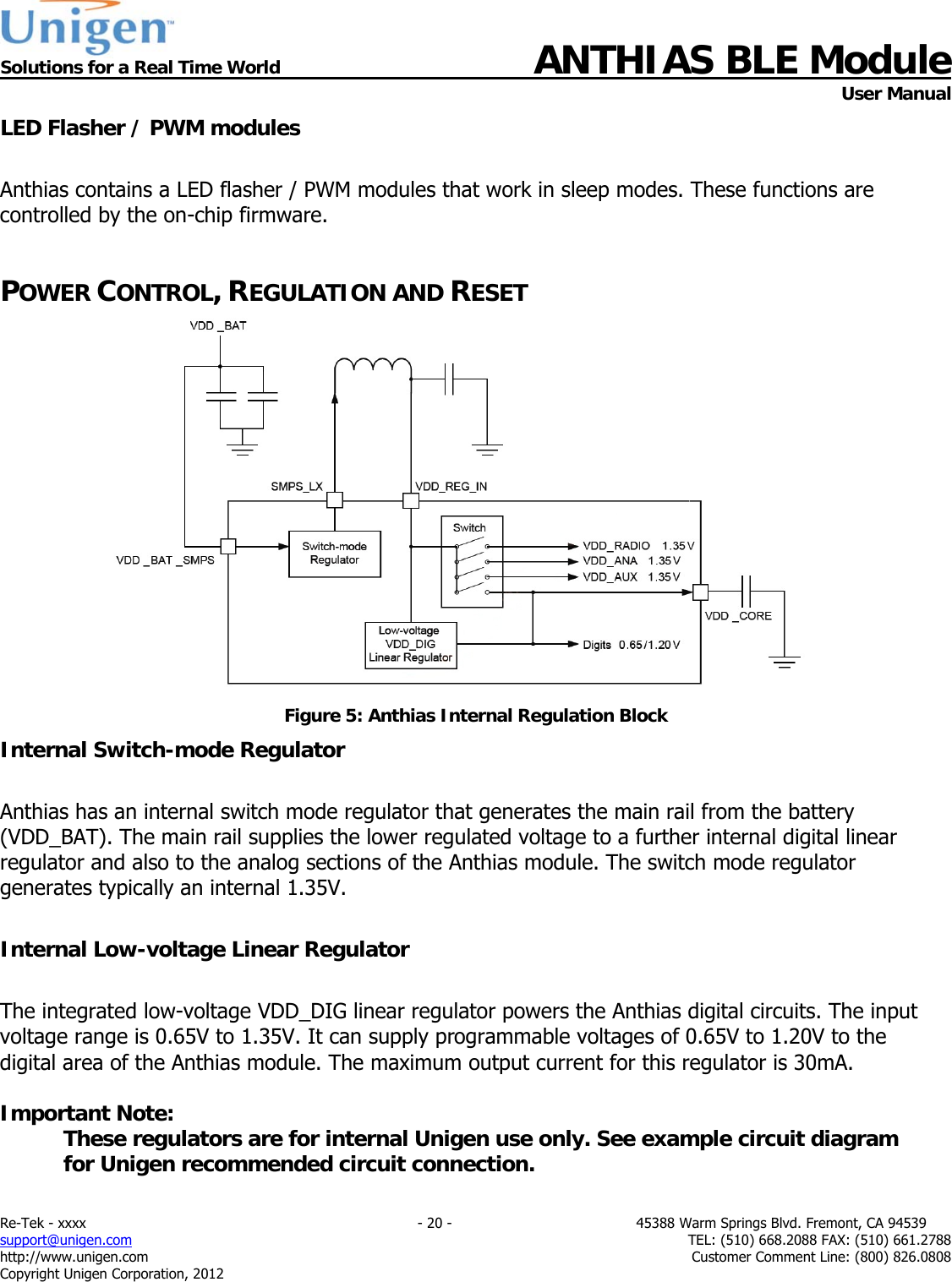
![Solutions for a Real Time World ANTHIAS BLE Module User Manual Re-Tek - xxxx - 22 - 45388 Warm Springs Blvd. Fremont, CA 94539 support@unigen.com TEL: (510) 668.2088 FAX: (510) 661.2788 http://www.unigen.com Customer Comment Line: (800) 826.0808 Copyright Unigen Corporation, 2012 The table below shows the possible UART settings for the ANTHIAS module. Table 10: Anthias UART Parameters Parameter Possible Values Baud Rate Minimum 1200 baud (≤2% Error) 9600 baud (≤1% Error) Maximum 2Mbaud (≤1% Error) Flow Control CTS/RTS Parity None, Odd or Even Number of stop bits 1 or 2 Bits per byte 8 Note: The maximum baud rate during Deep Sleep is 9600 baud. SPI Master Serial Flash Interface The SPI Serial Flash Interface is only available if Anthias is ordered and configured without the internal EEPROM option on the module. The SPI master memory interface in the Anthias module is overlaid on the internal I²C EEPROM interface and uses 3 other specific PIOs for the additional signaling. See the table on the next page for more details. PIO[2] is used to power the Serial Flash upon boot up to read the contents and load into RAM. After loading the contents, PIO[2] is de-asserted to shut down the Serial Flash for power savings. Figure 6: External Serial EEPROM Circuitry](https://usermanual.wiki/Unigen/UGWANBL2/User-Guide-1828523-Page-22.png)
![Solutions for a Real Time World ANTHIAS BLE Module User Manual Re-Tek - xxxx - 23 - 45388 Warm Springs Blvd. Fremont, CA 94539 support@unigen.com TEL: (510) 668.2088 FAX: (510) 661.2788 http://www.unigen.com Customer Comment Line: (800) 826.0808 Copyright Unigen Corporation, 2012 The table below shows the corresponding external Serial Flash signals when the external serial Flash option of the Anthias module is used to store the application code. Table 11: Anthias External Serial Flash Signals SPI Serial Flash Interface Pad Label Description FLASH_VDD 22 PIO_2 / I2C_SF_VDD Programmable I/O line or I²C Serial Flash power supply SF_DIN 9 PIO_3 / SF_DIN Programmable I/O line or SPI serial flash data (SF_DIN) input SF_CS# 10 PIO_4 / SF_CS# Programmable I/O line or SPI serial flash chip select (SF_CS#) SF_CLK 21 I2C_SCL / SF_CLK SPI serial flash clock output (SF_CLK). SF_DOUT 20 I2C_SDA / SF_DOUT SPI serial flash data output (SF_DOUT). Programming and Debug Interface Important Note: The Anthias module debug SPI interface is available in SPI slave mode to enable an external microcontroller to program and control the module, generally via libraries or tools supplied by CSR/Unigen. The protocol of this interface is proprietary. The 4 SPI debug lines directly support this function. The SPI programs, configures and debugs the Anthias module. It is required for firmware upgrade or debug. Ensure the 4 SPI signals are brought out to either test points or a header. If firmware upgrading is required in the field then this interface needs to be accessible externally. Take SPI_PIO#_SEL high to enable the SPI debug feature on PIO[8:5]. Anthias uses a 16-bit data and 16-bit address programming and debug interface. Transactions occur when the internal processor is running or is stopped. Data is written or read one word at a time, or the auto-increment feature is available for block access.](https://usermanual.wiki/Unigen/UGWANBL2/User-Guide-1828523-Page-23.png)