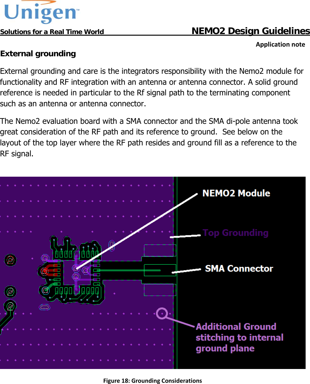
Unigen UGWC821R NEMO BLUETOOTH RADIO MODULE User Manual NEMO2 Design Guidelines
Unigen Corporation NEMO BLUETOOTH RADIO MODULE NEMO2 Design Guidelines
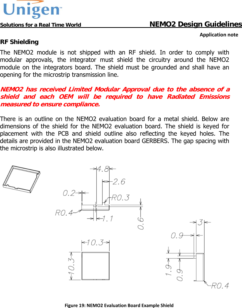
Unigen >
Contents
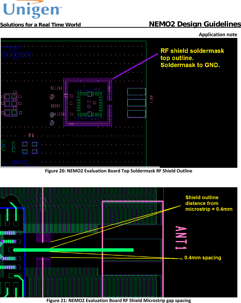
- 1. user manual
- 2. user manual design guidelines
user manual design guidelines
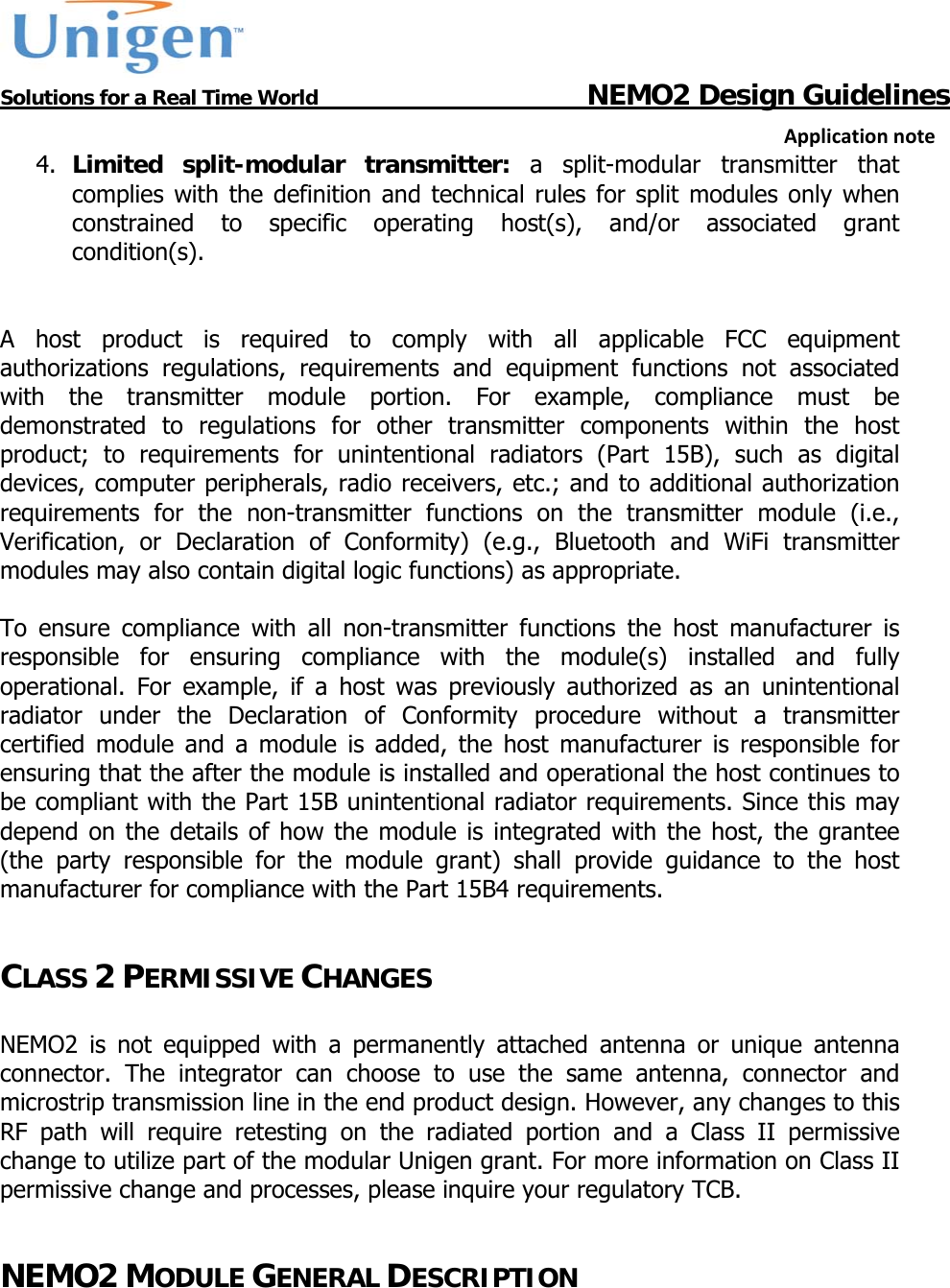
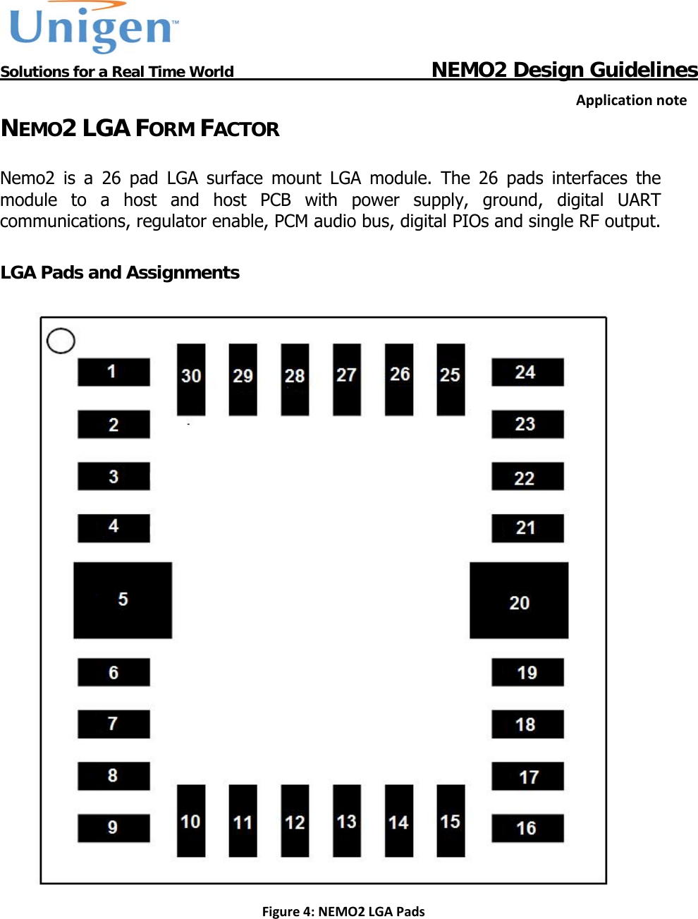
![Solutions for a Real Time World NEMO2 Design GuidelinesApplicationnoteTable1:NEMO2LGAPadDescription Pin Signal Name Type Description 1 CLK32K_IN Input 32.768kHz low power clock input 2 SDIO_SD_CSB Input SDIO Interface/Enable 3 SDIO_SD_CMD -- SDIO Interface 4 SDIO_SD_CLK -- SDIO Interface 5 GND -- Ground Reference 6 PIO(0) I/O I/O or WiFi- Coex signal 7 PIO(1) I/O I/O or WiFi- Coex signal 8 PIO(4) I/O I/O or WiFi- Coex signal 9 PIO(5) I/O I/O or WiFi- Coex signal 10 PIO(7) I/O I/O 11 GND -- Ground Reference 12 GND -- Ground Reference 13 ANT_OUT -- Antenna Output 14 GND -- Ground Reference 15 GND -- Ground Reference 16 PCM_CLK -- PCM Interface 17 PCM_OUT -- PCM Interface 18 PCM_IN -- PCM Interface 19 PCM_SYNC -- PCM Interface 20 GND -- Ground Reference 21 UART_RX/SDIO_DATA[2] I/O UART/SDIO_DATA Interface 22 UART_RTS/SDIO_DATA[1] I/O UART/SDIO_DATA Interface 23 UARTCTS/SDIO_DATA[3] I/O UART/SDIO_DATA Interface 24 UART_TX/SDIO_DATA[0] I/O UART/SDIO_DATA Interface 25 GND -- Ground Reference 26 BT_REG_CTRL_P PWR Internal Regulator Enable. 27 3V3 PWR PWR Supply 28 3V3 PWR PWR Supply 29 MODULE_RST_N Input Module Reset 30 VDD_RF -- Output of Internal Regulator Note: Active Low signals are designated with an '_N' suffix, and Active High signals are designated with an '_P' suffix.](https://usermanual.wiki/Unigen/UGWC821R.user-manual-design-guidelines/User-Guide-1722661-Page-13.png)

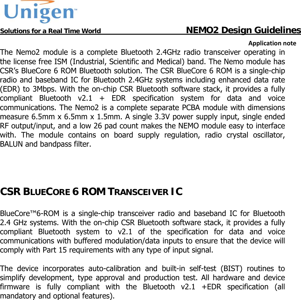
![Solutions for a Real Time World NEMO2 Design GuidelinesApplicationnoteSoftware and Host Nemo2 is intended to operate with a host. The host will communicate to the module via the physical communication interfaces, UART/SDIO, to control the modules RF operating behavior. The host shall run the Bluetooth Upper software protocol stack operate Nemo2 in Bluetooth modes only. Nemo2 is not intended to operate without a host and Bluetooth protocol stack. The Nemo2 software interface is based on the Bluetooth Host Controller Interface Transport Layer specification (HCI). For more details on the Bluetooth HCI protocol layer, please see the latest Bluetooth Specification (3.0+HS), volume 4 and the section pertaining to Host Controller Interface [Transport Layer] Figure13:NEMO2BluetoothSoftwareStackArchitecture](https://usermanual.wiki/Unigen/UGWC821R.user-manual-design-guidelines/User-Guide-1722661-Page-23.png)