Vitelcom Mobile Technology USA TSM501 Single Band CDMA Cellular Phone User Manual
Vitelcom Mobile Technology USA, Inc. Single Band CDMA Cellular Phone
UserManual.wiki
>
Vitelcom Mobile Technology USA
>
TSM501 User Manual
>
Service manual
Contents
1.
User manual
2.
Service manual
Service manual
Navigation menu
Upload a User Manual
Namespaces
Wiki Guide
HTML
PDF
Info
Views
User Manual
Discussion / Help
Navigation
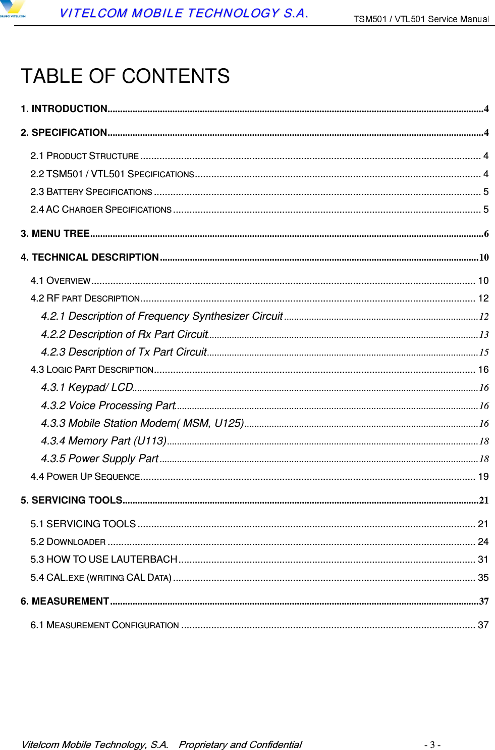
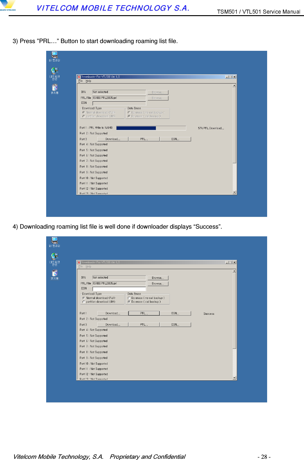
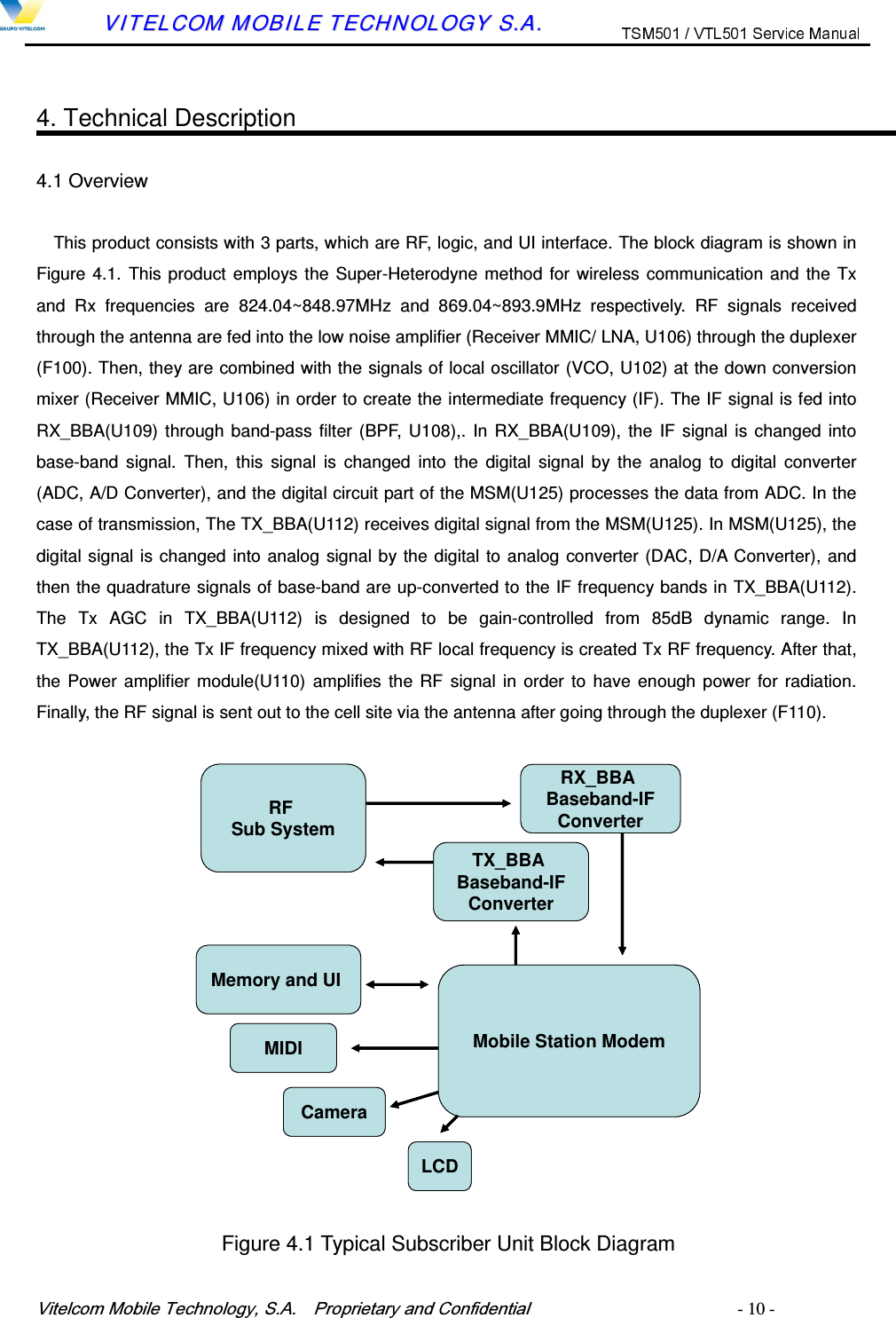
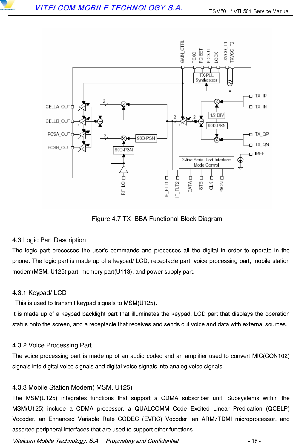
![9LWHOFRP0RELOH7HFKQRORJ\6$ 3URSULHWDU\DQG&RQILGHQWLDO - 4 - VVIITTEELLCCOOMM MMOOBBIILLEE TTEECCHHNNOOLLOOGGYY SS..AA.. 1. Introduction This manual provides the technical information to support the service activities of TSM501 / VTL501 model, which operates on Single mode Digital CDMA Telephone. This manual is supplied in the electronic format for easy distribution and reference. Also refer to the following documents: -. Service Drawings of TSM501 / VTL501 model phone (Schematic diagrams and Parts layout) -. Service Part List of TSM501 / VTL501 model phone -. Owner’s Operating Manuals of TSM501 / VTL501 model phone 2. Specification This chapter provides the product configuration and product specifications of TSM501 / VTL501 model, which operates on Single mode Digital CDMA Telephone and accessories 2.1 Product Structure [Table 2.1] Standard Package ITEM TYPES 1 Handheld Portable Telephone TSM501 / VTL501 2 Lithium Ion Battery(850mAh) TSM501 / VTL501 3 AC Charger TSM501 / VTL501 T.C 4 Earphone-Mic Earphone-Mic is offered by VITELCOM 5 Handstrap Handstrap is offered by VITELCOM 6 Owner’s Operating Manual TSM501 / VTL501 Manuals 2.2 TSM501 / VTL501 Specifications ITEM 800MHz Band 1 Radio Frequency TX: 824 to 849MHz RX:869 to 894MHz 2 Number of Channels 832 3 Duplex Spacing 45MHz 4 Digital Mode 4.1 Channel Spacing 1.23MHz 4.2 Frequency Stability +/-300Hz 4.3 RF Output Power 24dBm](https://usermanual.wiki/Vitelcom-Mobile-Technology-USA/TSM501.Service-manual/User-Guide-540123-Page-4.png)
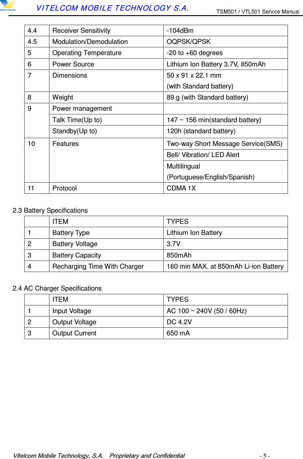
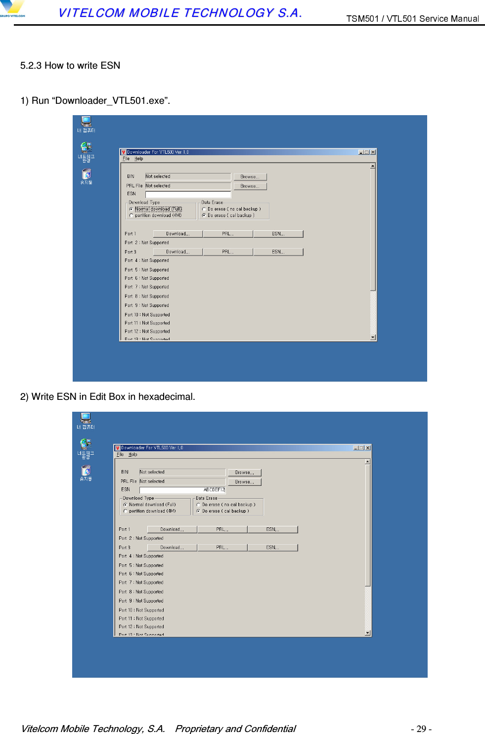
![9LWHOFRP0RELOH7HFKQRORJ\6$ 3URSULHWDU\DQG&RQILGHQWLDO - 17 - VVIITTEELLCCOOMM MMOOBBIILLEE TTEECCHHNNOOLLOOGGYY SS..AA.. MSM(U125) Internal Block 1) ARM Microprocessor Subsystem The MSM(U125) uses an embedded ARM7TDMI microprocessor. The ARM7TDMI microprocessor, through the system software, controls most of the functionality for the Mobile Station, including control of the external peripherals such as the keypad, LCD display, RAM and ROM/FLASH(U113) devices. 2) RF Interface This block communicates with the MSM(U125) RF, IF and Analog Base-band circuitry. 3) CDMA Subsystem: Digital IS-2000 Signal Processing. Searcher engine Demodulating fingers Combining block Frame de-interleaver Viterbi decoder Reverse link subsystem 4) UART (Universal Asynchronous Receiver Transmitter) Two identical UARTs, UART1 has dedicated pins while UART2 share multiplexed pins with the Auxiliary PCM CODEC interface. 5) Vocoder Subsystem The MSM(U125)’s QDSP2000 supports EVRC and QCELP13K vocoders. In addition, the QDSP2000 has modules to support the following audio functions; DTMF tone generation, DTMF tone detection, Tx/Rx volume controls, Tx/Rx automatic gain control(AGC), Rx Automatic Volume Control(AVC), Ear Seal Echo Canceller(ESEC), Acoustic Echo Canceller(AEC), Noise Suppression(NS), and programmable, 13-tap, Type-I, FIR, Tx/Rx compensation filters. The MSM(U125)’s integrated ARM7TDMI processor downloads the firmware into the QDSP2000 and configures QDSP2000 to support the desired functionality. 6) General Purpose Interface Bus The MSM(U125) has 48 general-purpose bi-directional input/output pins (GPIO_INT[47:0]) that double as general-purpose interrupt inputs. Some of the GPIO_INT pins have alternate functions supported on them. The alternate functions include, USB interface, additional RAM, ROM/Flash(U113), general-purpose chip selects, parallel LCD interface, and a UART interface. The function of these pins is documented in the various software releases. 7) Serial Bus Interface](https://usermanual.wiki/Vitelcom-Mobile-Technology-USA/TSM501.Service-manual/User-Guide-540123-Page-17.png)
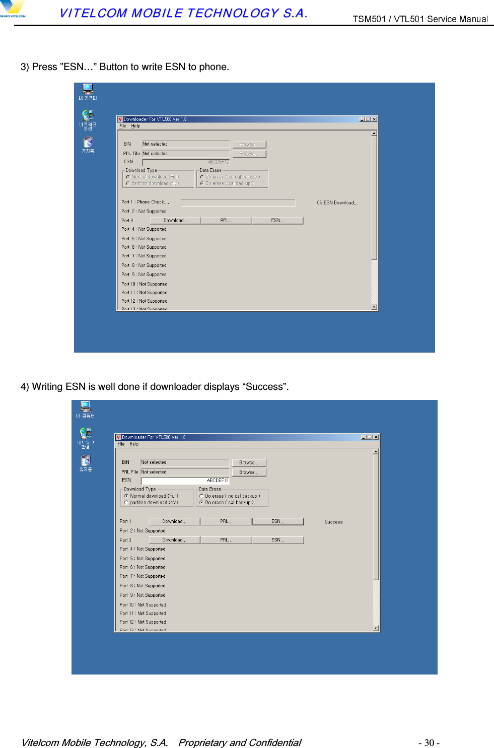
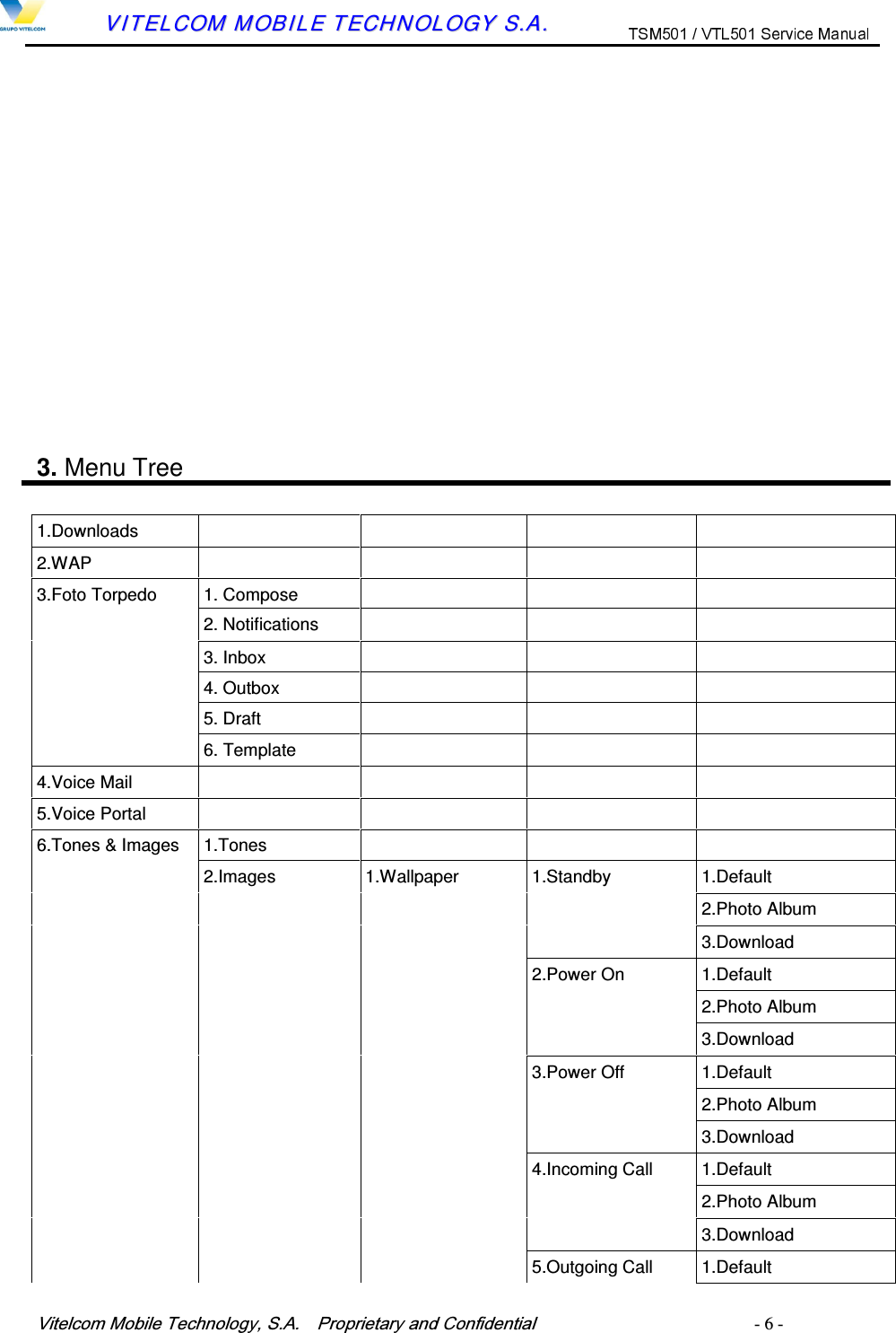
![9LWHOFRP0RELOH7HFKQRORJ\6$ 3URSULHWDU\DQG&RQILGHQWLDO - 18 - VVIITTEELLCCOOMM MMOOBBIILLEE TTEECCHHNNOOLLOOGGYY SS..AA.. This interface is specifically designed to be a quick, low pin count control protocol for Qualcomm’s TX_BBA(U112) can be configured for different operating modes and configured for minimum power consumption, extending battery life in standby mode. 8) User Interface MSM(U125) user interface comprises digital connections to the subscriber unit ringer transducer, keypad and LCD display. 9) Mode Select and JTAG Interfaces The Mode select inputs to the MSM(U125) determine overall mode of the ASIC. The options under the control of the Mode select inputs are Native Mode which is the normal subscriber unit operation and ICE Mode in which the on-chip ARM microprocessor is disabled, allowing off-chip emulation by the ICE unit. 4.3.4 Memory Part (U113) Components: Combination Memory [Flash Memory (128Mbit) + SRAM (32Mbit)] 1) Flash Memory (128Mbit) Stores telephone’s main and sub programs. Memory for source code : 12Mbyte . Memory for NV parameter value , SMS, Phone Book, Download data, PIMS data, camera data.. etc : 4Mbyte. - Code Flash memory: 8MB (4Mbit x 16), Random Access Time is 70ns - Data Flash memory: 8MB (4Mbit x 16), Random Access Time is 70ns 2) SRAM (32Mbit) Stores changes in other person’s system parameter and Data Task data Buffer and stack of each task. - SRAM: 4MB (2Mbit x 16), Max. Access Time is 70ns 4.3.5 Power Supply Part Power is supplied by battery or external source of which range is 3.2~4.2V voltage. It is sent to LDO (Low dropout regulator), which supply 2.8V for Logic power.](https://usermanual.wiki/Vitelcom-Mobile-Technology-USA/TSM501.Service-manual/User-Guide-540123-Page-18.png)
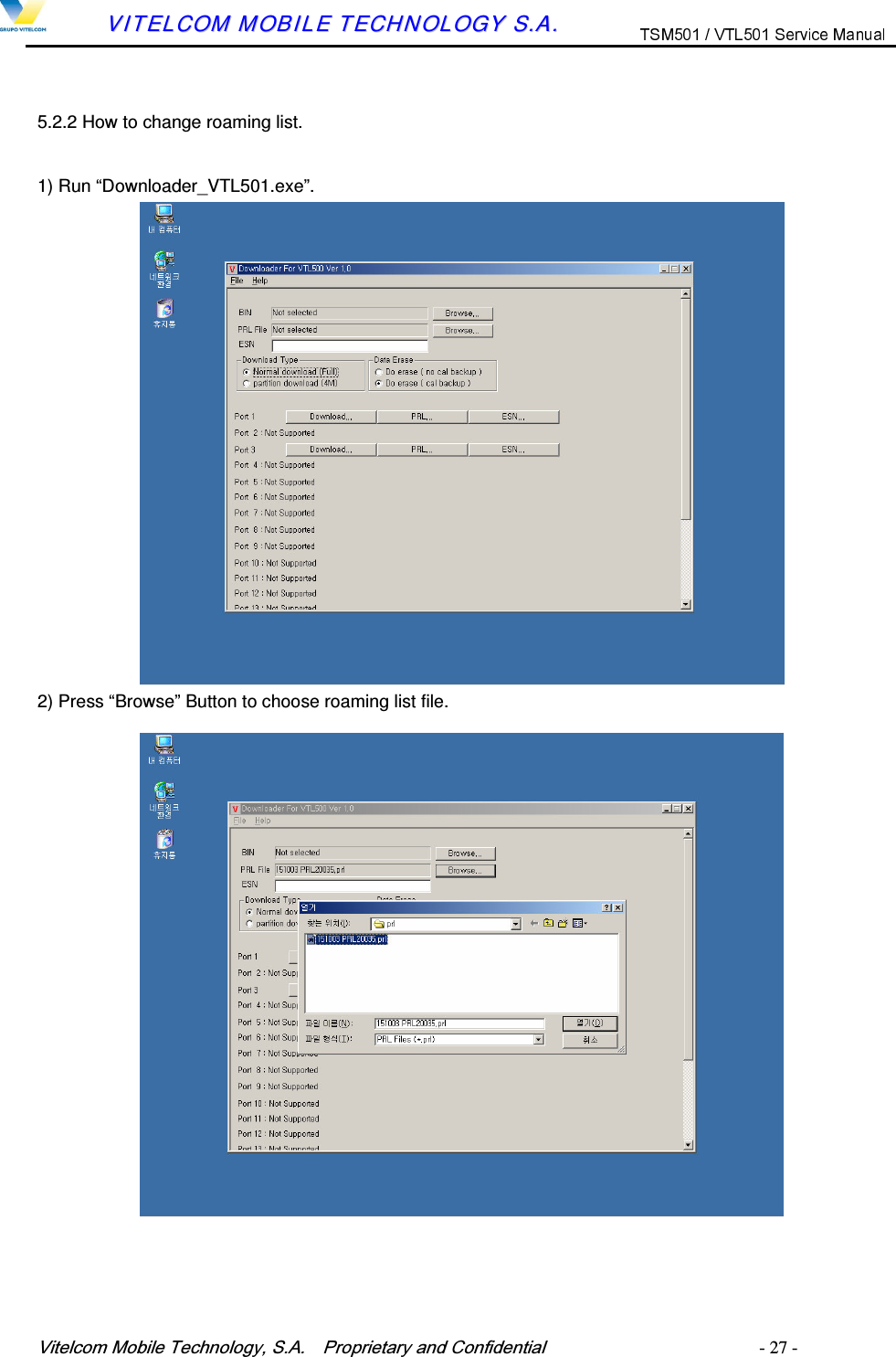
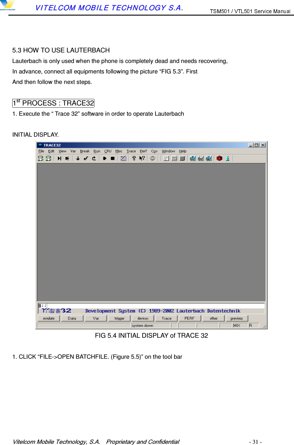
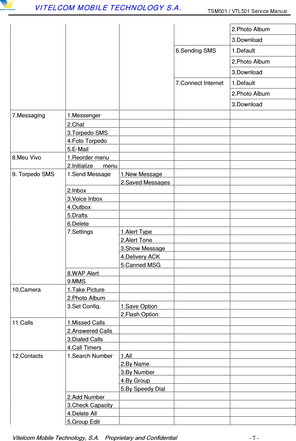
![9LWHOFRP0RELOH7HFKQRORJ\6$ 3URSULHWDU\DQG&RQILGHQWLDO - 19 - VVIITTEELLCCOOMM MMOOBBIILLEE TTEECCHHNNOOLLOOGGYY SS..AA.. Figure 4.8 VTL501 Logic Part Block Diagram 4.4 Power Up Sequence This section describes the steps how the TSM501 / VTL501 phone wakes up. Place a Battery Pack The battery pack, which the protection circuit is implemented, is placed into the phone. Press and Hold [END] Key The Power on circuit (SW124) generates the control voltage to be used for U6. Regulators Activated U6 feeds 2.8V to MSM (U125), LCD U6 feeds 2.8V to Flash ROM / SRAM (U113) and others. U6 feeds 2.8V to VCTCXO(U104) and others.](https://usermanual.wiki/Vitelcom-Mobile-Technology-USA/TSM501.Service-manual/User-Guide-540123-Page-19.png)